EN
EN  ES
ES  DE
DE  FR
FR  IT
IT  ZH
ZH  JA
JA  PT
PT  TR
TR  KO
KO  PL
PL  AR
AR Category: Application Notes
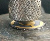
Coating Tribology of Gold on Quartz Crystal Substrate
The QCM works based on the piezoelectric properties of the quartz crystal. It measures the mass change on the surface down to 0.1 nanogram during material deposition by detecting variations in the resonance frequency of the crystal. Due to the extreme sensitive and accurate characteristics of the QCM, it is critical to ensure that the two electrodes on both sides of the quartz plate possess good wear resistance. Any mass loss on the metal electrodes caused by wear can lead to significant error in the measurement. Therefore, reliable and accurate wear evaluation using a Tribometer is important for quality control and R&D of QCMs.

3D Topography With Image Overlay of PCB
The more sophisticated electronic design and layout of semiconductor chips, circuits and systems requires high precision manufacturing and superior quality control. Unlike other techniques such as touch probes or interferometry, the Nanovea 3D Non-Contact Profilometer, using axial chromatism, can measure nearly any material surface. Nano through macro range is obtained during surface profile measurement with zero influence from sample reflectivity, absorption and high surface angles. This is ideal for surface inspection of the PCB assembly (PCBA), which contains a variety of electronic components of different materials, reflectivity and fine features. Moreover, the non-contact profiling technique measures the surface features without touching the PCBA, avoiding the risk of damaging the delicate circuits and electronic components due to sliding of the probe stylus. The combination of high precision, high speed, non-contact and user friendliness makes the Nanovea Profilometer an ideal tool for PCBA inspection.

Copper Wire Coating Failure Using Tribology
The surface quality of copper wire is critical in its service performance and lifetime. The micro defects in the wire surface may lead to excessive wear, crack initiation and propagation, and inadequate solderability. Proper surface treatment can remove surface defects that are generated during wire drawing, and improve the corrosion, wear and scratch resistance of the copper wire. Many applications such as aerospace and commercial airliner require copper wires to behave in a controlled manner to prevent unexpected equipment failure. Quantifiable and reliable measurements are in need in order to quantitatively evaluate the wear and scratch resistance of the copper wire surface.

Mechanical Property Broadview Mapping Tool
Seen above is an example of Nanovea’s patent pending Broadview Map Selection Tool. This new tool allows users easy selection of any location on a broad stitched surface view of the sample. Additionally, the user can select all testing parameters at each location, either for a one test or a multi-tests mapping. All locations and test parameters can be saved in easily retrievable recipes. This significant advancement provides fast & friendly Nano through Macro mechanical property studies. Learn more in this months app note: Mechanical Property Mapping
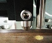
Wood Hardness & Elastic Modulus Using Microindentation
In this application, the Nanovea Mechanical Tester, in microindentation mode is used to compare the mechanical properties of three different types of wood. We would like to showcase the capacity of Nanovea Mechanical Tester in performing hardness and Young’s modulus on wood samples with high precision and reproducibility.

Surface Finish Inspection of Wood Using 3D Profilometry
In this study, the Nanovea ST500 Profilometer, equipped with a line sensor and integrated optical microscope, is used for surface finish inspection of wood samples, namely Cherry and Walnut. We showcases the capacity of Nanovea non-contact profilometer in providing fast and precise 3D finish measurement and comprehensive in-depth analysis for comparative review.

Fossil Mechanical Properties using Nanoindentation
In this application, the Nanovea Mechanical Tester, in Nanoindentation mode is used to map fossil mechanical properties of different locations of an ammonite fossil sample. We would like to showcase the capacity of Nanovea Mechanical Tester in performing nanoindentation mapping on a fossil sample with high precision and reproducibility.

Rock Tribology Using Tribometer
In this study, we simulated and compared the tribological properties of two types of rocks to showcase the capacity of Nanovea Tribometer in measuring the coefficient of friction and wear rate of rock tribology in a controlled and monitored manner.
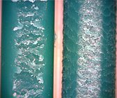
Wear & Friction Of Polymer Belts Using Tribometer
In this study, we simulated and compared the wear behaviors of belts with different surface texture to showcase the capacity of Nanovea Tribometer in simulating the wear process of the belt in a controlled and monitored manner.
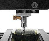
DMA Frequency Sweep On Polymer Using Nanoindentation
In this application, the Nanovea Mechanical Tester, in Nanoindentation mode is used to study the
viscoelastic properties of a polished tire sample at different DMA frequencies.