Monthly Archives: March 2018

Mechanical Properties of Silicon Carbide Wafer Coatings
Understanding the mechanical properties of silicon carbide wafer coatings is critical. The fabrication process for microelectronic devices can have over 300 different processing steps and can take anywhere from six to eight weeks. During this process, the wafer substrate must be able to withstand the extreme conditions of manufacturing, since a failure at any step would result in the loss of time and money. The testing of hardness, adhesion/scratch resistance and COF/wear rate of the wafer must meet certain requirements in order to survive the conditions imposed during the manufacturing and application process to insure a failure will not occur.
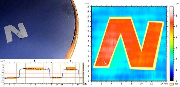
Wafer Coating Thickness Measurement Using 3D Profilometry
Wafer Coating Thickness Measurement is critical. Silicon wafers are widely used in the making of integrated circuits and other micro devices used in a vast number of industries. A constant demand for thinner and smoother wafers and wafer coatings makes the Nanovea 3D non-contact Profilometer a great tool to quantify coating thickness and roughness of just about any surface. The measurements in this article were taken from a coated wafer sample in order to demonstrate the capabilities of our 3D Non-Contact Profilometer.