USA/GLOBAL: +1-949-461-9292
EUROPE: +39-011-3052-794
CONTACT US

Category: Scratch Testing | Cohesive Failure


Weld Surface Inspection Using a Portable 3D Profilometer

WELd surface inspection

using a portable 3d profilometer

Prepared by

CRAIG LEISING

INTRODUCTION

It may become critical for a particular weld, typically done by visual inspection, to be investigated with an extreme level of precision. Specific areas of interest for precise analysis include surface cracks, porosity and unfilled craters, regardless of subsequent inspection procedures. Weld characteristics such as dimension/shape, volume, roughness, size etc. can all be measured for critical evaluation.

IMPORTANCE OF 3D NON-CONTACT PROFILOMETER FOR WELD SURFACE INSPECTION

Unlike other techniques such as touch probes or interferometry, the NANOVEA 3D Non-Contact Profilometer, using axial chromatism, can measure nearly any surface, sample sizes can vary widely due to open staging and there is no sample preparation needed. Nano through macro range is obtained during surface profile measurement with zero influence from sample reflectivity or absorption, has advanced ability to measure high surface angles and there is no software manipulation of results. Easily measure any material: transparent, opaque, specular, diffusive, polished, rough etc. The 2D and 2D capabilities of the NANOVEA Portable Profilometers make them ideal instruments for full complete weld surface inspection both in the lab and in the field.

MEASUREMENT OBJECTIVE

In this application, the NANOVEA JR25 Portable Profiler is used to measure the surface roughness, shape and volume of a weld, as well as the surrounding area. This information can provide critical information to properly investigate the quality of the weld and weld process.

NANOVEA

JR25

TEST RESULTS

The image below shows the full 3D view of the weld and the surrounding area along with the surface parameters of the weld only. The 2D cross section profile is shown below.

the sample

With the above 2D cross section profile removed from the 3D, dimensional information of the weld is calculated below. Surface area and volume of material calculated for the weld only below.

 HOLEPEAK
SURFACE1.01 mm214.0 mm2
VOLUME8.799e-5 mm323.27 mm3
MAX DEPTH/HEIGHT0.0276 mm0.6195 mm
MEAN DEPTH/HEIGHT 0.004024 mm 0.2298 mm

CONCLUSION

In this application, we have shown how the NANOVEA 3D Non-Contact Profiler can precisely characterize critical characteristics of a weld and the surrounding surface area. From the roughness, dimensions and volume, a quantitative method for quality and repeatability can be determined and or further investigated. Sample welds, such as the example in this app note, can be easily analyzed, with a standard tabletop or portable NANOVEA Profiler for in-house or field testing

NOW, LET'S TALK ABOUT YOUR APPLICATION

Industrial Coatings Scratch and Wear Evaluation

INDUSTRIAL COATING

SCRATCH AND WEAR EVALUATION USING A TRIBOMETER

Prepared by

DUANJIE LI, PhD & ANDREA HERRMANN

INTRODUCTION

Acrylic urethane paint is a type of fast-dry protective coating widely used in a variety of industrial applications, such as floor paint, auto paint, and others. When used as floor paint, it can serve areas with heavy foot and rubber-wheel traffic, such as walkways, curbs and parking lots.

IMPORTANCE OF SCRATCH AND WEAR TESTING FOR QUALITY CONTROL

Traditionally, Taber abrasion tests were carried out to evaluate the wear resistance of acrylic urethane floor paint according to the ASTM D4060 standard. However, as mentioned in the standard, “For some materials, abrasion tests utilizing the Taber Abraser may be subject to variation due to changes in the abrasive characteristics of the wheel during testing.”1 This may result in poor reproducibility of test results and create difficulty in comparing values reported from different laboratories. Moreover, in Taber abrasion tests, abrasion resistance is calculated as loss in weight at a specified number of abrasion cycles. However, acrylic urethane floor paints have a recommended dry film thickness of 37.5-50 μm2.

The aggressive abrasion process by Taber Abraser can quickly wear through the acrylic urethane coating and create mass loss to the substrate leading to substantial errors in the calculation of the paint weight loss. The implant of abrasive particles in the paint during the abrasion test also contributes to errors. Therefore, a well-controlled quantifiable and reliable measurement is crucial to ensure reproducible wear evaluation of the paint. In addition, the scratch test allows users to detect premature adhesive/cohesive failures in real-life applications.

MEASUREMENT OBJECTIVE

In this study, we showcase that NANOVEA Tribometers and Mechanical Testers are ideal for evaluation and quality control of industrial coatings.

The wear process of acrylic urethane floor paints with different topcoats is simulated in a controlled and monitored manner using the NANOVEA Tribometer. Micro scratch testing is used to measure the load required to cause cohesive or adhesive failure to the paint.

NANOVEA T100

The Compact Pneumatic Tribometer

NANOVEA PB1000

The Large Platform Mechanical Tester

TEST PROCEDURE

This study evaluates four commercially available water-based acrylic floor coatings that have the same primer (basecoat) and different topcoats of the same formula with a small alternation in the additive blends for the purpose of enhancing durability. These four coatings are identified as Samples A, B, C and D.

WEAR TEST

The NANOVEA Tribometer was applied to evaluate the tribological behavior, e.g. coefficient of friction, COF, and wear resistance. A SS440 ball tip (6 mm dia., Grade 100) was applied against the tested paints. The COF was recorded in situ. The wear rate, K, was evaluated using the formula K=V/(F×s)=A/(F×n), where V is the worn volume, F is the normal load, s is the sliding distance, A is the cross-sectional area of the wear track, and n is the number of revolution. Surface roughness and wear track profiles were evaluated by the NANOVEA Optical Profilometer, and the wear track morphology was examined using optical microscope.

WEAR TEST PARAMETERS

NORMAL FORCE

20 N

SPEED

15 m/min

DURATION OF TEST

100, 150, 300 & 800 cycles

SCRATCH TEST

The NANOVEA Mechanical Tester equipped with a Rockwell C diamond stylus (200 μm radius) was used to perform progressive load scratch tests on the paint samples using the Micro Scratch Tester Mode. Two final loads were used: 5 N final load for investigating paint delamination from the primer, and 35 N for investigating primer delamination from the metal substrates. Three tests were repeated at the same testing conditions on each sample to ensure reproducibility of the results.

Panoramic images of the whole scratch lengths were automatically generated and their critical failure locations were correlated with the applied loads by the system software. This software feature facilitates users to perform analysis on the scratch tracks any time, rather than having to determine the critical load under the microscope immediately after the scratch tests.

SCRATCH TEST PARAMETERS

LOAD TYPEProgressive
INITIAL LOAD0.01 mN
FINAL LOAD5 N / 35 N
LOADING RATE10 / 70 N/min
SCRATCH LENGTH3 mm
SCRATCHING SPEED, dx/dt6.0 mm/min
INDENTER GEOMETRY120º cone
INDENTER MATERIAL (tip)Diamond
INDENTER TIP RADIUS200 μm

WEAR TEST RESULTS

Four pin-on-disk wear tests at different number of revolutions (100, 150, 300 and 800 cycles) were performed on each sample in order to monitor the evolution of wear. The surface morphology of the samples were measured with a NANOVEA 3D Non-Contact Profiler to quantify the surface roughness prior to conducting wear testing. All samples had a comparable surface roughness of approximately 1 μm as displayed in FIGURE 1. The COF was recorded in situ during the wear tests as shown in FIGURE 2. FIGURE 4 presents the evolution of wear tracks after 100, 150, 300 and 800 cycles, and FIGURE 3 summarized the average wear rate of different samples at different stages of the wear process.


Compared with a COF value of ~0.07 for the other three samples, Sample A exhibits a much higher COF of ~0.15 at the beginning, which gradually increases and gets stable at ~0.3 after 300 wear cycles. Such a high COF accelerates the wear process and creates a substantial amount of paint debris as indicated in FIGURE 4 – the topcoat of Sample A has started to be removed in the first 100 revolutions. As shown in FIGURE 3, Sample A exhibits the highest wear rate of ~5 μm2/N in the first 300 cycles, which slightly decreases to ~3.5 μm2/N due to the better wear resistance of the metal substrate. The topcoat of Sample C starts to fail after 150 wear cycles as shown in FIGURE 4, which is also indicated by the increase of COF in FIGURE 2.


In comparison, Sample B and Sample D show enhanced tribological properties. Sample B maintains a low COF throughout the whole test – the COF slightly increases from~0.05 to ~0.1. Such a lubricating effect substantially enhances its wear resistance – the topcoat still provides superior protection to the primer underneath after 800 wear cycles. The lowest average wear rate of only ~0.77 μm2/N is measured for Sample B at 800 cycles. The topcoat of Sample D starts to delaminate after 375 cycles, as reflected by the abrupt increase of COF in FIGURE 2. The average wear rate of Sample D is ~1.1 μm2/N at 800 cycles.


Compared to the conventional Taber abrasion measurements, NANOVEA Tribometer provides well-controlled quantifiable and reliable wear assessments that ensure reproducible evaluations and quality control of commercial floor/auto paints. Moreover, the capacity of in situ COF measurements allow users to correlate the different stages of a wear process with the evolution of COF, which is critical in improving fundamental understanding of the wear mechanism and tribological characteristics of various paint coatings.

FIGURE 1: 3D morphology and roughness of the paint samples.

FIGURE 2: COF during pin-on-disk tests.

FIGURE 3: Evolution of wear rate of different paints.

FIGURE 4: Evolution of wear tracks during the pin-on-disk tests.

WEAR TEST RESULTS

FIGURE 5 shows the plot of normal force, frictional force and true depth as a function of scratch length for Sample A as an example. An optional acoustic emission module can be installed to provide more information. As the normal load linearly increases, the indentation tip gradually sinks into the tested sample as reflected by the progressive increase of true depth. The variation in the slopes of frictional force and true depth curves can be used as one of the implications that coating failures start to occur.

FIGURE 5: Normal force, frictional force and true depth as a function of scratch length for scratch test of Sample A with a maximum load of 5 N.

FIGURE 6 and FIGURE 7 show the full scratches of all four paint samples tested with a maximum load of 5 N and 35 N, respectively. Sample D required a higher load of 50 N to delaminate the primer. Scratch tests at 5 N final load (FIGURE 6) evaluate the cohesive/adhesive failure of the top paint, while the ones at 35 N (FIGURE 7) assess the delamination of the primer. The arrows in the micrographs indicate the point at which the top coating or the primer start to be completely removed from the primer or the substrate. The load at this point, so called Critical Load, Lc, is used to compare the cohesive or adhesive properties of the paint as summarized in Table 1.


It is evident that the paint Sample D has the best interfacial adhesion – exhibiting the highest Lc values of 4.04 N at paint delamination and 36.61 N at primer delamination. Sample B shows the second best scratch resistance. From the scratch analysis, we show that optimization of the paint formula is critical to the mechanical behaviors, or more specifically, scratch resistance and adhesion property of acrylic floor paints.

Table 1: Summary of critical loads.

FIGURE 6: Micrographs of full scratch with 5 N maximum load.

FIGURE 7: Micrographs of full scratch with 35 N maximum load.

CONCLUSION

Compared to the conventional Taber abrasion measurements, the NANOVEA Mechanical Tester and Tribometer are superior tools for evaluation and quality control of commercial floor and automotive coatings. The NANOVEA Mechanical Tester in Scratch mode can detect adhesion/cohesion problems in a coating system. The NANOVEA Tribometer provides well-controlled quantifiable and repeatable tribological analysis on wear resistance and coefficient of friction of the paints.


Based on the comprehensive tribological and mechanical analyses on the water based acrylic floor coatings tested in this study, we show that Sample B possesses the lowest COF and wear rate and the second best scratch resistance, while Sample D exhibits the best scratch resistance and second best wear resistance. This assessment allows us to evaluate and select the best candidate targeting the needs in different application environments.


The Nano and Micro modules of the NANOVEA Mechanical Tester all include ISO and ASTM compliant indentation, scratch and wear tester modes, providing the widest range of testing available for paint evaluation on a single module. The NANOVEA Tribometer offers precise and repeatable wear and friction testing using ISO and ASTM compliant rotative and linear modes, with optional high temperature wear, lubrication and tribo-corrosion modules available in one pre-integrated system. NANOVEA’s unmatched range is an ideal solution for determining the full range of mechanical/tribological properties of thin or thick, soft or hard coatings, films and substrates, including hardness, Young’s modulus, fracture toughness, adhesion, wear resistance and many others. Optional NANOVEA Non-Contact Optical Profilers are available for high resolution 3D imaging of scratchs and wear tracks in addition to other surface measurements such as roughness.

NOW, LET'S TALK ABOUT YOUR APPLICATION

Titanium Nitride Coating Scratch Test

TITANIUM NITRIDE COATING SCRATCH TEST

QUALITY CONTROL INSPECTION

Prepared by

DUANJIE LI, PhD

INTRODUCTION

The combination of high hardness, excellent wear resistance, corrosion resistance and inertness makes titanium nitride (TiN) an ideal protective coating for metal components in various industries. For example, the edge retention and corrosion resistance of a TiN coating can substantially increase the work efficiency and extend the service life of machine tooling such as razor blades, metal cutters, injection molds and saws. Its high hardness, inertness and non-toxicity make TiN a great candidate for applications in medical devices including implants and surgical instruments.

IMPORTANCE OF TiN COATING SCRATCH TESTING

Residual stress in protective PVD/CVD coatings plays a critical role in the performance and mechanical integrity of the coated component. The residual stress derives from several major sources, including growth stress, thermal gradients, geometric constraints and service stress¹. The thermal expansion mismatch between the coating and the substrate created during coating deposition at elevated temperatures leads to high thermal residual stress. Moreover, TiN coated tools are often used under very high concentrated stresses, e.g. drill bits and bearings. It is critical to developing a reliable quality control process to quantitatively inspect the cohesive and adhesive strength of protective functional coatings.

[1] V. Teixeira, Vacuum 64 (2002) 393–399.

MEASUREMENT OBJECTIVE

In this study, we showcase that the NANOVEA Mechanical Testers in Scratch Mode are ideal for assessing the cohesive/adhesive strength of protective TiN coatings in a controlled and quantitative manner.

NANOVEA

PB1000

TEST CONDITIONS

The NANOVEA PB1000 Mechanical Tester was used to perform coating scratch tests on three TiN coatings using the same test parameters as summarized below:

LOADING MODE: Progressive Linear

INITIAL LOAD

0.02 N

FINAL LOAD

10 N

LOADING RATE

20 N/min

SCRATCH LENGTH

5 mm

INDENTER TYPE

Sphero-Conical

Diamond, 20 μm radius

RESULTS & DISCUSSION

FIGURE 1 shows the recorded evolution of penetration depth, coefficient of friction (COF) and acoustic emission during the test. The full micro scratch tracks on the TiN samples are shown in FIGURE 2. The failure behaviors at different critical loads are displayed in FIGURE 3, where critical load Lc1 is defined as the load at which the first sign of cohesive crack occurs in the scratch track, Lc2 is the load after which repeated spallation failures take place, and Lc3 is the load at which the coating is completely removed from the substrate. The critical load (Lc) values for the TiN coatings are summarized in FIGURE 4.

The evolution of penetration depth, COF and acoustic emission provides insight into the mechanism of the coating failure at different stages, which are represented by the critical loads in this study. It can be observed that Sample A and Sample B exhibit comparable behavior during the scratch test. The stylus progressively penetrates into the sample to a depth of ~0.06 mm and the COF gradually increases to ~0.3 as the normal load increases linearly at the beginning of the coating scratch test. When the Lc1 of ~3.3 N is reached, the first sign of chipping failure occurs. This is also reflected in the first large spikes in the plot of penetration depth, COF and acoustic emission. As the load continues to increase to Lc2 of ~3.8 N, further fluctuation of the penetration depth, COF and acoustic emission takes place. We can observe continuous spallation failure present on both sides of the scratch track. At the Lc3, the coating completely delaminates from the metal substrate under the high pressure applied by the stylus, leaving the substrate exposed and unprotected.

In comparison, Sample C exhibits lower critical loads at different stages of the coating scratch tests, which is also reflected in the evolution of penetration depth, coefficient of friction (COF) and acoustic emission during the coating scratch test. Sample C possesses an adhesion interlayer with lower hardness and higher stress at the interface between the top TiN coating and the metal substrate compared to Sample A and Sample B.

This study demonstrates the importance of proper substrate support and coating architecture to the quality of the coating system. A stronger interlayer can better resist deformation under a high external load and concentration stress, and thus enhance the cohesive and adhesive strength of the coating/substrate system.

FIGURE 1: Evolution of penetration depth, COF and acoustic emission of the TiN samples.

FIGURE 2: Full scratch track of the TiN coatings after the tests.

FIGURE 3: TiN coating failures under different critical loads, Lc.

FIGURE 4: Summary of critical load (Lc) values for the TiN coatings.

CONCLUSION

In this study, we showcased that the NANOVEA PB1000 Mechanical Tester performs reliable and accurate scratch tests on TiN-coated samples in a controlled and closely monitored manner. Scratch measurements allow users to quickly identify the critical load at which typical cohesive and adhesive coating failures occur. Our instruments are superior quality control tools that can quantitatively inspect and compare the intrinsic quality of a coating and the interfacial integrity of a coating/substrate system. A coating with a proper interlayer can resist large deformation under a high external load and concentration stress, and enhance the cohesive and adhesive strength of a coating/substrate system.

The Nano and Micro modules of a NANOVEA Mechanical Tester all include ISO and ASTM compliant indentation, scratch and wear tester modes, providing the widest and most user-friendly range of testing available in a single system. NANOVEA’s unmatched range is an ideal solution for determining the full range of mechanical properties of thin or thick, soft or hard coatings, films and substrates, including hardness, Young’s modulus, fracture toughness, adhesion, wear-resistance and many others.

NOW, LET'S TALK ABOUT YOUR APPLICATION

Adhesion Properties of Gold Coating on Quartz Crystal Substrate


Adhesion Properties of Gold Coating

on Quartz Crystal Substrate

Prepared by

DUANJIE LI, PhD

INTRODUCTION

The Quartz Crystal Microbalance (QCM) is an extremely sensitive mass sensor capable of making precise measurements of small mass in the nanogram range. QCM measures the mass change on the surface through detecting variations in resonance frequency of the quartz crystal with two electrodes affixed to each side of the plate. The capacity of measuring extreme small weight makes it a key component in a variety of research and industrial instruments to detect and monitor the variation of mass, adsorption, density, and corrosion, etc.

IMPORTANCE OF SCRATCH TEST FOR QCM

As an extremely accurate device, the QCM measures the mass change down to 0.1 nanogram. Any mass loss or delamination of the electrodes on the quartz plate will be detected by the quartz crystal and cause significant measurement errors. As a result, the intrinsic quality of the electrode coating and the interfacial integrity of the coating/substrate system play an essential role in performing accurate and repeatable mass measurement. The Micro scratch test is a widely used comparative measurement to evaluate the relative cohesion or adhesion properties of coatings based on comparison of the critical loads at which failures appear. It is a superior tool for reliable quality control of QCMs.

MEASUREMENT OBJECTIVE

In this application, the NANOVEA Mechanical Tester, in Micro Scratch Mode, is used to evaluate the cohesive & adhesive strength of the gold coating on the quartz substrate of a QCM sample. We would like to showcase the capacity of the NANOVEA Mechanical Tester in performing micro scratch tests on a delicate sample with high precision and repeatability.

NANOVEA

PB1000

TEST CONDITIONS

The NANOVEA PB1000 Mechanical Tester was used to perform the micro scratch tests on a QCM sample using the test parameters summarized below. Three scratches were performed to ensure reproducibility of the results.

LOAD TYPE: Progressive

INITIAL LOAD

0.01 N

FINAL LOAD

30 N

ATMOSPHERE: Air 24°C

SLIDING SPEED

2 mm/min

SLIDING DISTANCE

2 mm

RESULTS & DISCUSSION

The full micro scratch track on the QCM sample is shown in FIGURE 1. The failure behaviors at different critical loads are displayed in FIGURE 2, where critical load, LC1 is defined as the load at which the first sign of adhesive failure occurs in the scratch track, LC2 is the load after which repetitive adhesive failures take place, and LC3 is the load at which the coating is completely removed from the substrate. It can be observed that little chipping takes place at LC1 of 11.15 N, the first sign of coating failure. 

As the normal load continues to increase during the micro scratch test, repetitive adhesive failures occur after LC2 of 16.29 N. When LC3 of 19.09 N is reached, the coating completely delaminates from the quartz substrate. Such critical loads can be used to quantitatively compare the cohesive and adhesive strength of the coating and select the best candidate for targeted applications.

FIGURE 1: Full micro scratch track on the QCM sample.

FIGURE 2: Micro scratch track at different critical loads.

FIGURE 3 plots the evolution of friction coefficient and depth that may provide more insight in the progression of coating failures during the micro scratch test.

FIGURE 3: Evolution of COF and Depth during the micro scratch test.

CONCLUSION

In this study, we showcased that the NANOVEA Mechanical Tester performs reliable and accurate micro scratch tests on a QCM sample. By applying linearly increased loads in a controlled and closely monitored fashion, the scratch measurement allows users to identify the critical load at which typical cohesive and adhesive coating failure occurs. It provides a superior tool to quantitatively evaluate and compare the intrinsic quality of the coating and the interfacial integrity of the coating/substrate system for QCM.

The Nano, Micro or Macro modules of the NANOVEA Mechanical Tester all include ISO and ASTM compliant indentation, scratch and wear tester modes, providing the widest and most user friendly range of testing available in a single system. NANOVEA‘s unmatched range is an ideal solution for determining the full range of mechanical properties of thin or thick, soft or hard coatings, films and substrates, including hardness, Young’s modulus, fracture toughness, adhesion, wear resistance and many others.

In addition, an optional 3D non-contact profiler and AFM module are available for high resolution 3D imaging of indentation, scratch and wear track in addition to other surface measurements, such as roughness and warpage.

NOW, LET'S TALK ABOUT YOUR APPLICATION

Wear and Scratch Evaluation of Surface Treated Copper Wire


Importance of Wear and Scratch Evaluation of Copper Wire

Copper has a long history of use in electric wiring since the invention of the electromagnet and telegraph. Copper wires are applied in a wide range of electronic equipment such as panels, meters, computers, business machines, and appliances thanks to its corrosion resistance, solderability, and performance at elevated temperatures up to 150°C. Approximately half of all mined copper is used for manufacturing electrical wire and cable conductors.

Copper wire surface quality is critical to application service performance and lifetime. Micro defects in wires may lead to excessive wear, crack initiation and propagation, decreased conductivity, and inadequate solderability. Proper surface treatment of copper wires removes surface defects generated during wire drawing improving corrosion, scratch, and wear resistance. Many aerospace applications with copper wires require controlled behavior to prevent unexpected equipment failure. Quantifiable and reliable measurements are needed to properly evaluate the wear and scratch resistance of the copper wire surface.


Measurement Objective

In this application we simulate a controlled wear process of different copper wire surface treatments. Scratch testing measures the load required to cause failure on the treated surface layer. This study showcases the Nanovea Tribometer and Mechanical Tester as ideal tools for evaluation and quality control of electric wires.


Test Procedure and Procedures

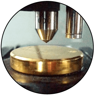
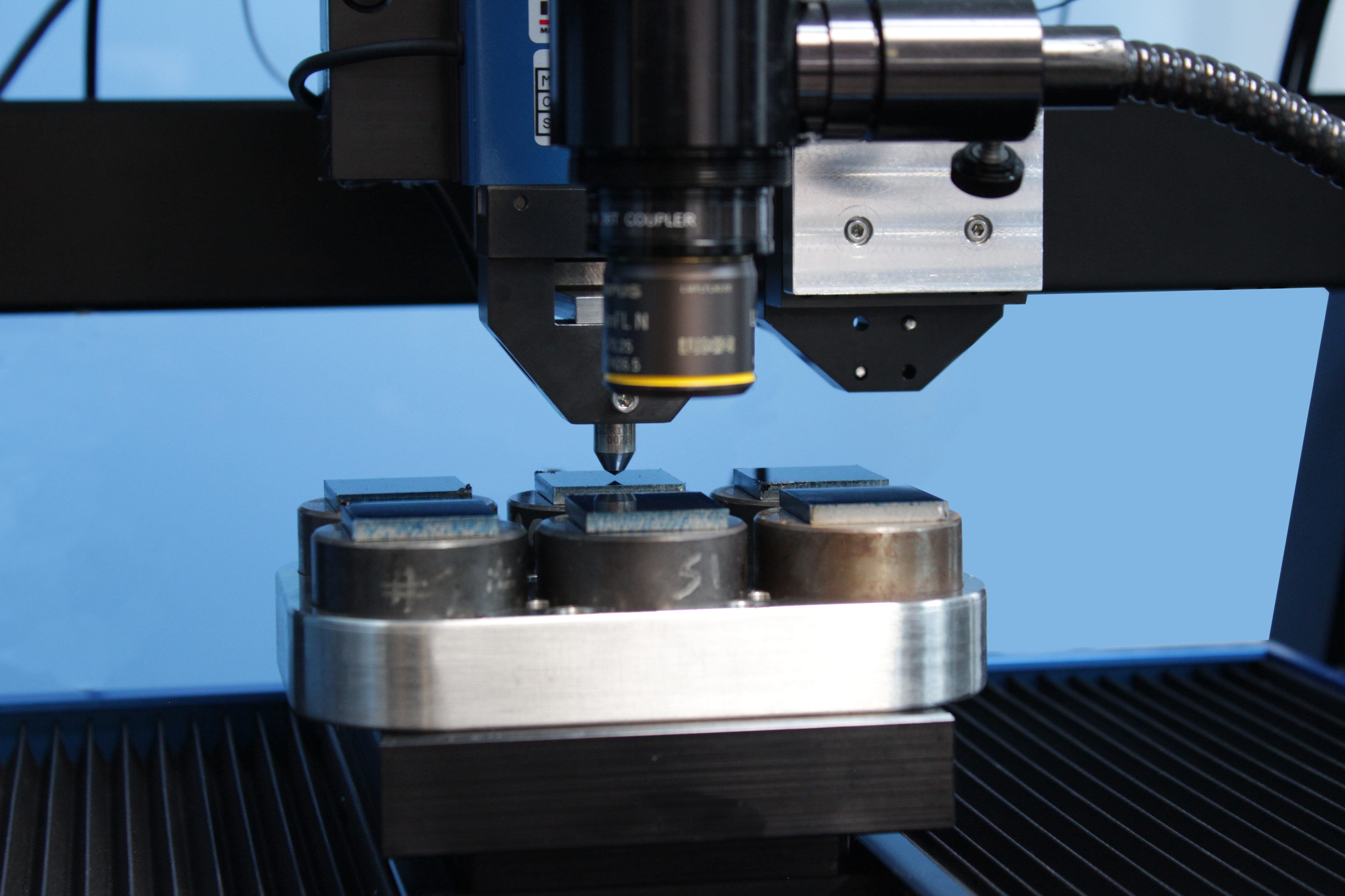
Coefficient of friction (COF) and wear resistance of two different surface treatments on copper wires (Wire A and Wire B) were evaluated by the Nanovea tribometer using a linear reciprocating wear module. An Al₂O₃ ball (6 mm diameter) is the counter material used in this application. The wear track was examined using Nanovea’s 3D non-contact profilometer. Test parameters are summarized in Table 1.

A smooth Al₂O₃ ball as a counter material was used as an example in this study. Any solid material with different shape and surface finish can be applied using a custom fixture to simulate the actual application situation.


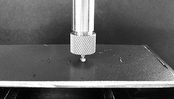
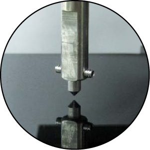
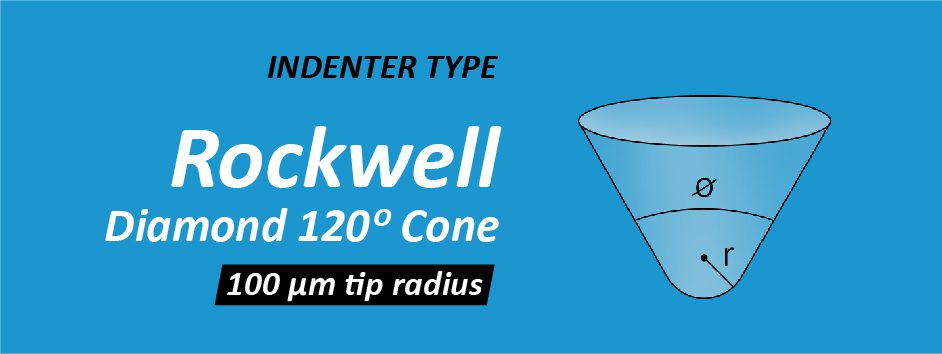
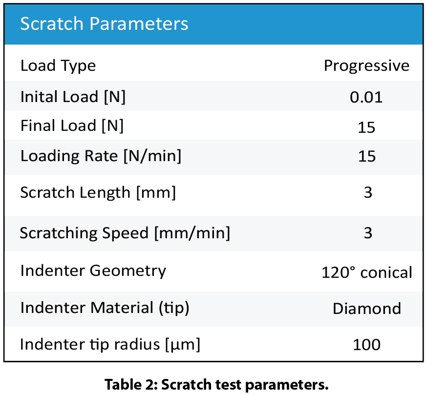
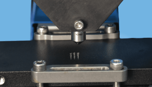
Nanovea’s mechanical tester equipped with a Rockwell C diamond stylus (100 μm radius) performed progressive load scratch tests on the coated wires using micro scratch mode. Scratch test parameters and tip geometry are shown in Table 2.


Results and Discussion

Wear of copper wire: 
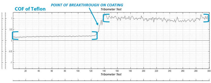
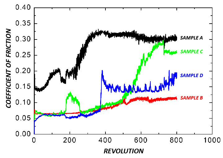
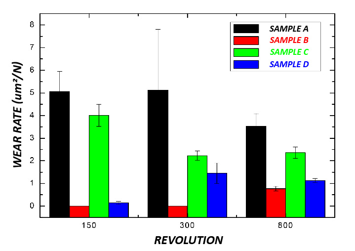
Figure 2 shows COF evolution of the copper wires during wear tests. Wire A shows a stable COF of ~0.4 throughout the wear test while wire B exhibits a COF of ~0.35 in the first 100 revolutions and progressively increases to ~0.4.


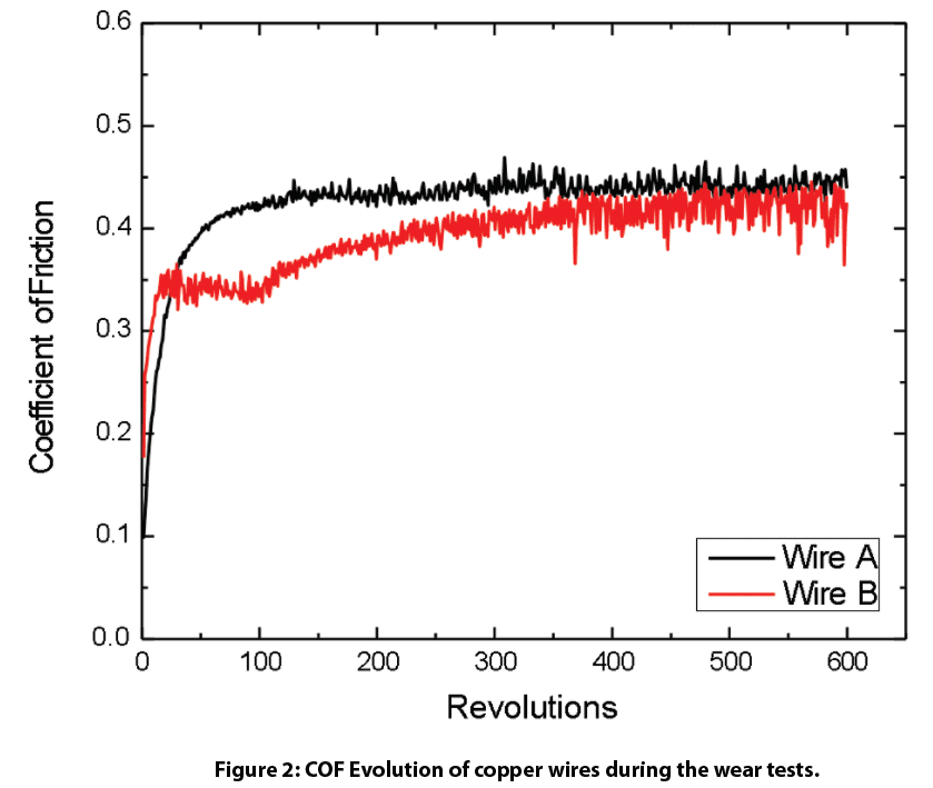
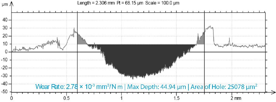
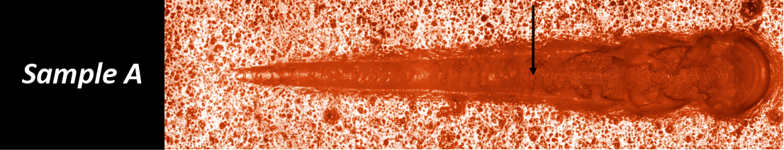
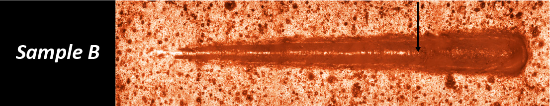
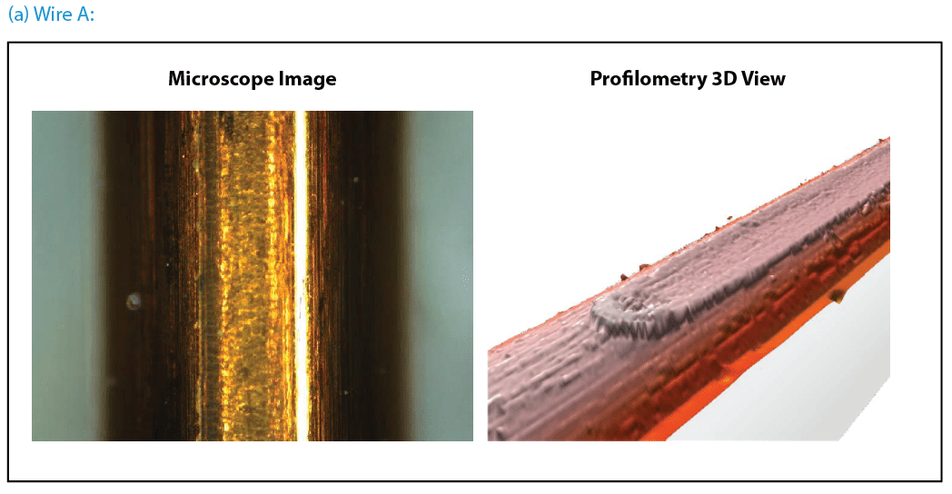
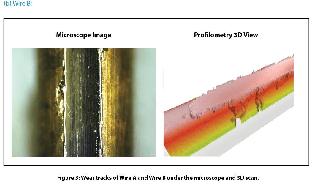
Figure 3 compares wear tracks of the copper wires after tests. Nanovea’s 3D non-contact profilometer offered superior analysis of the detailed morphology of wear tracks. It allows direct and accurate determination of the wear track volume by providing a fundamental understanding of the wear mechanism. Wire B’s surface has signi¬ficant wear track damage after a 600-revolution wear test. The profilometer 3D view shows the surface treated layer of Wire B removed completely which substantially accelerated the wear process. This left a flattened wear track on Wire B where copper substrate is exposed. This may result in significantly shortened lifespan of electrical equipment where Wire B is used. In comparison, Wire A exhibits relatively mild wear shown by a shallow wear track on the surface. The surface treated layer on Wire A did not remove like the layer on Wire B under the same conditions.


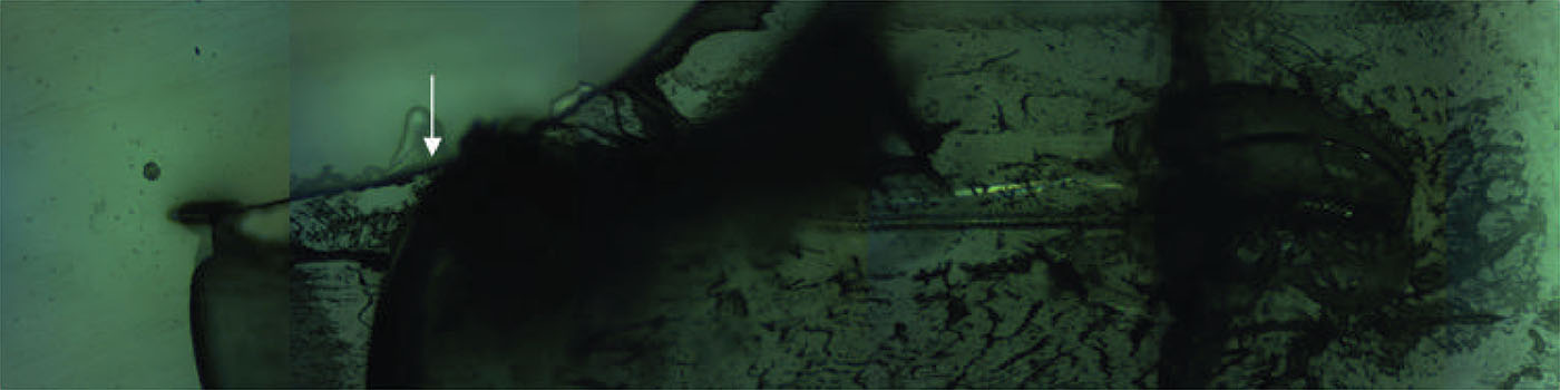
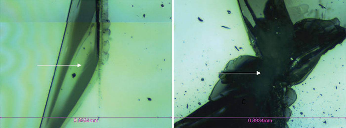
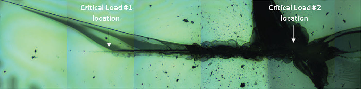
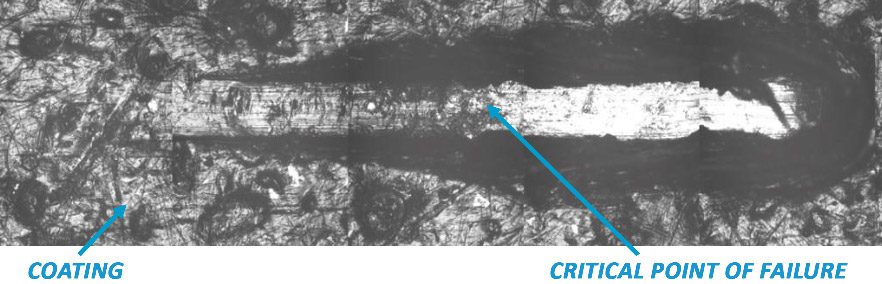
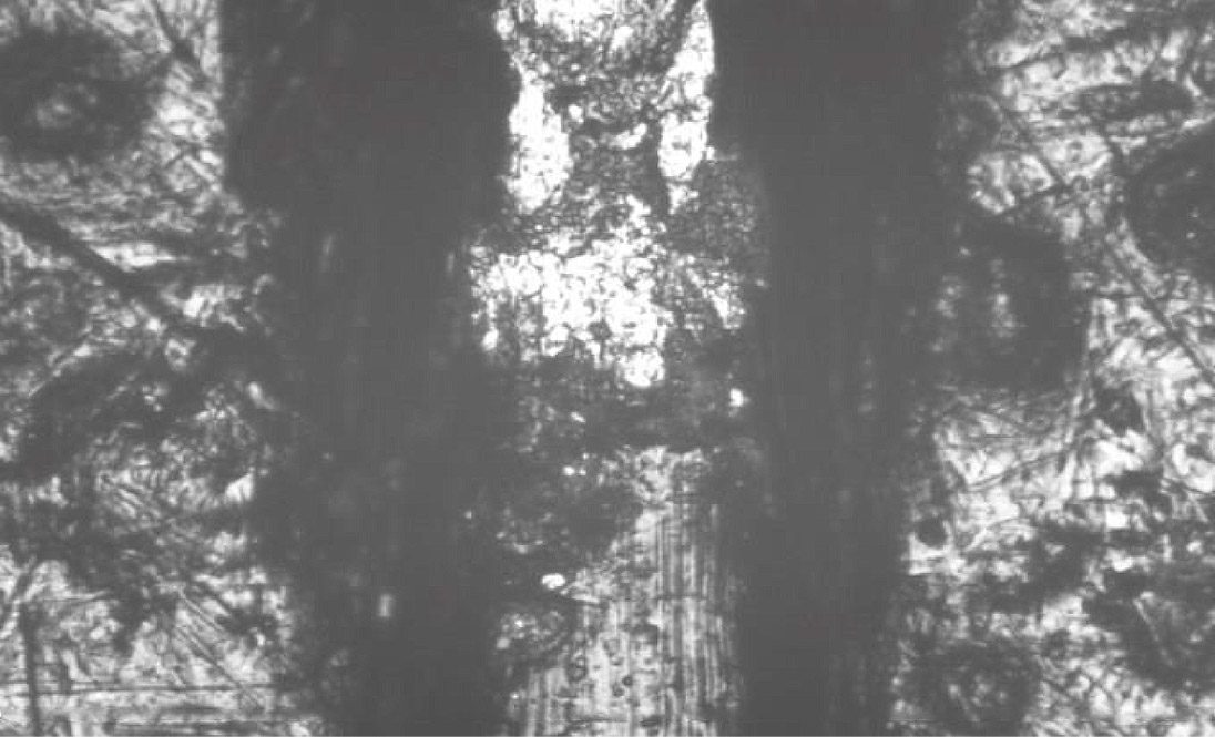
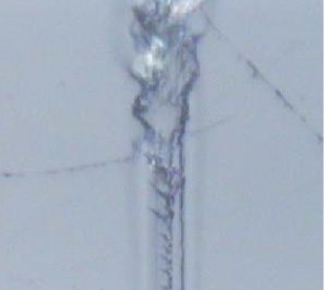
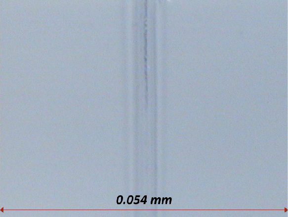
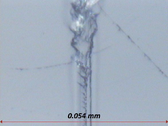
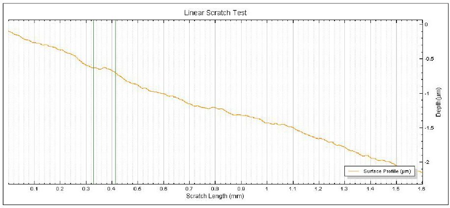
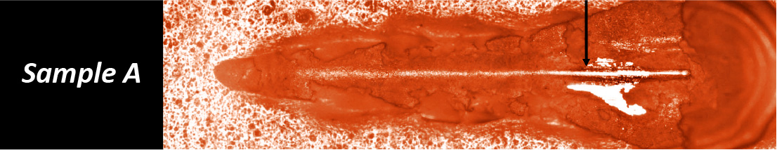
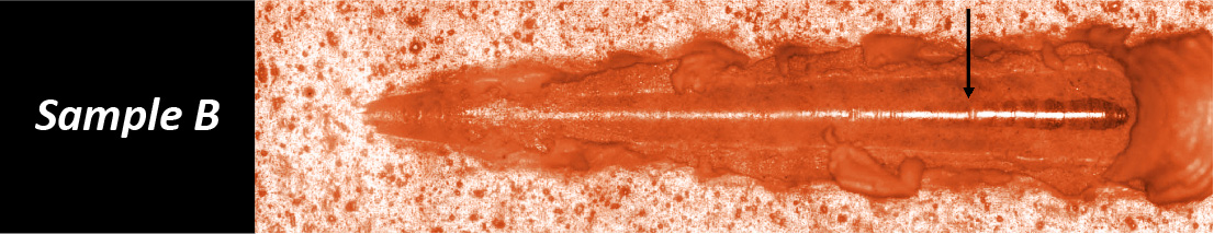
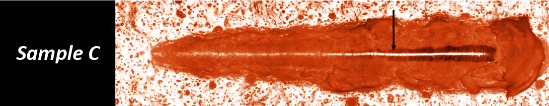
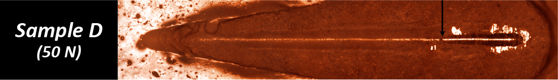
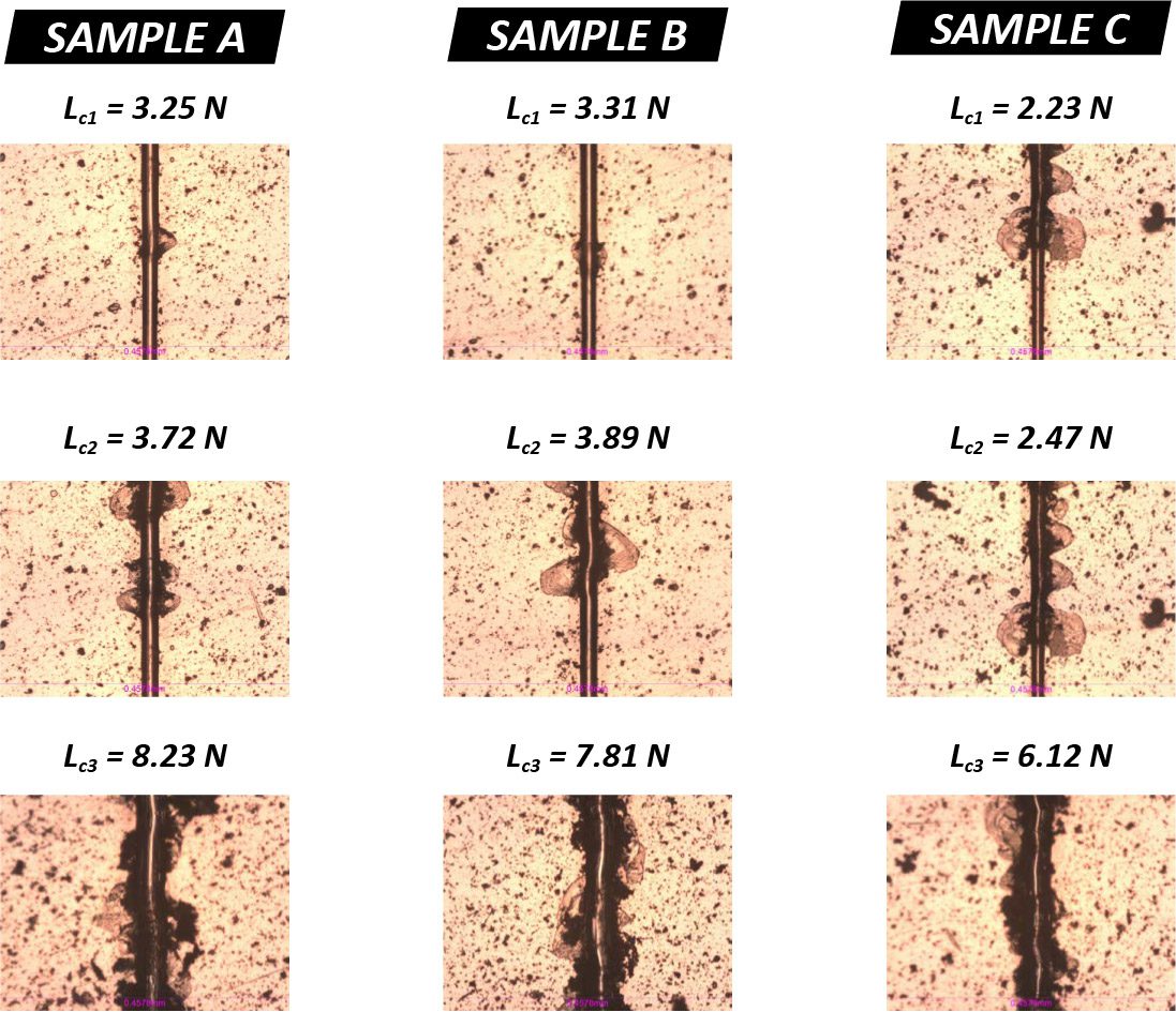
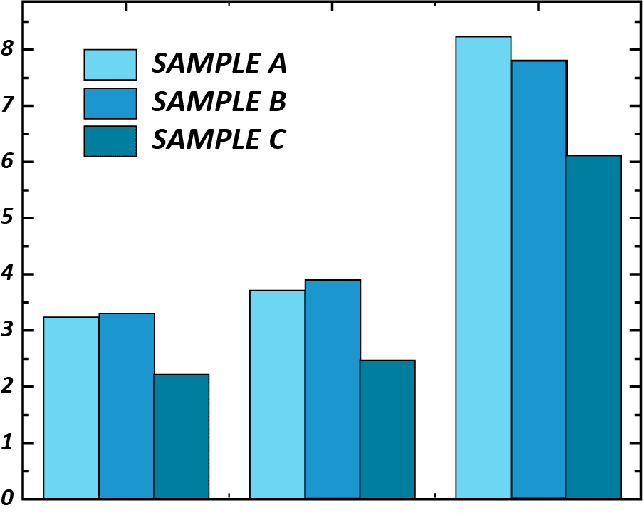
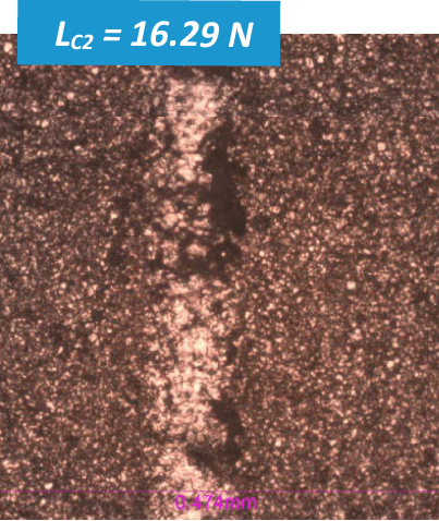
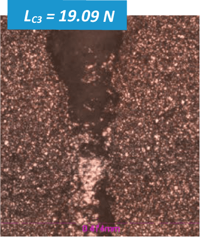
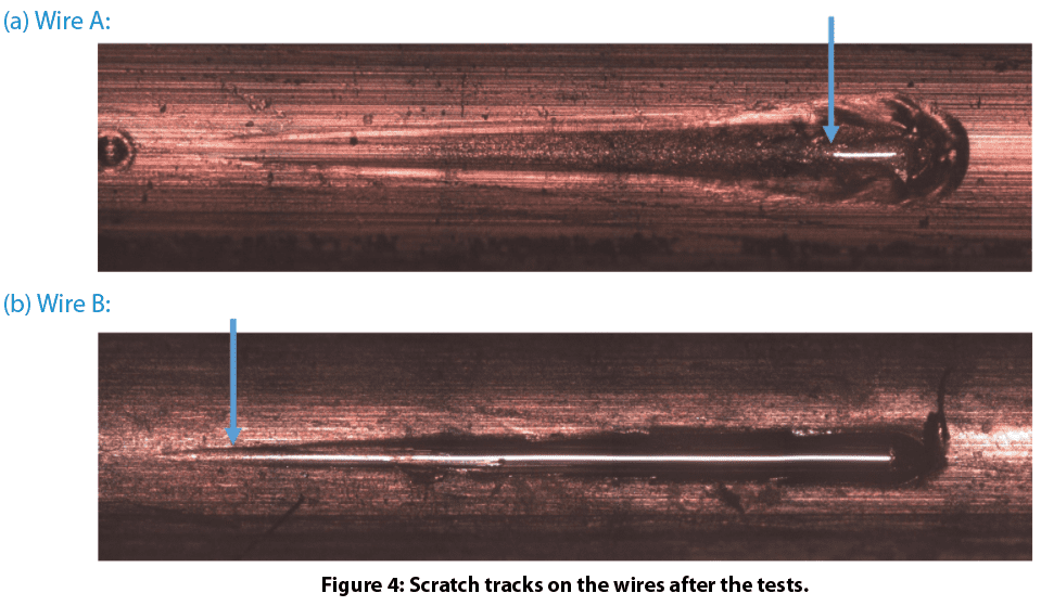
Scratch resistance of the copper wire surface: 
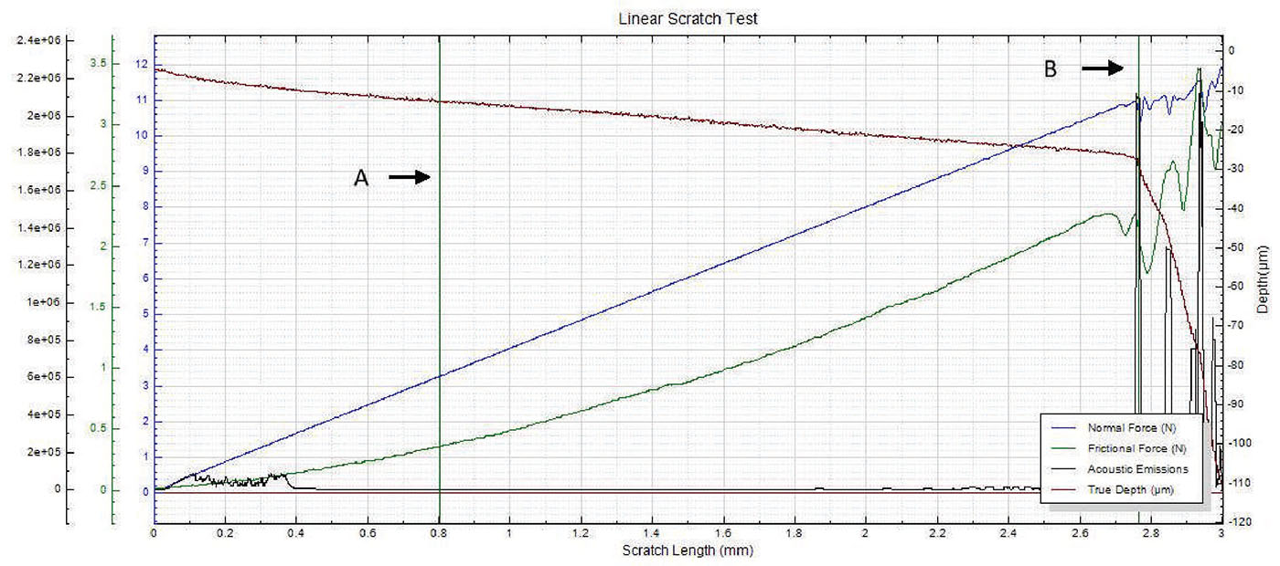
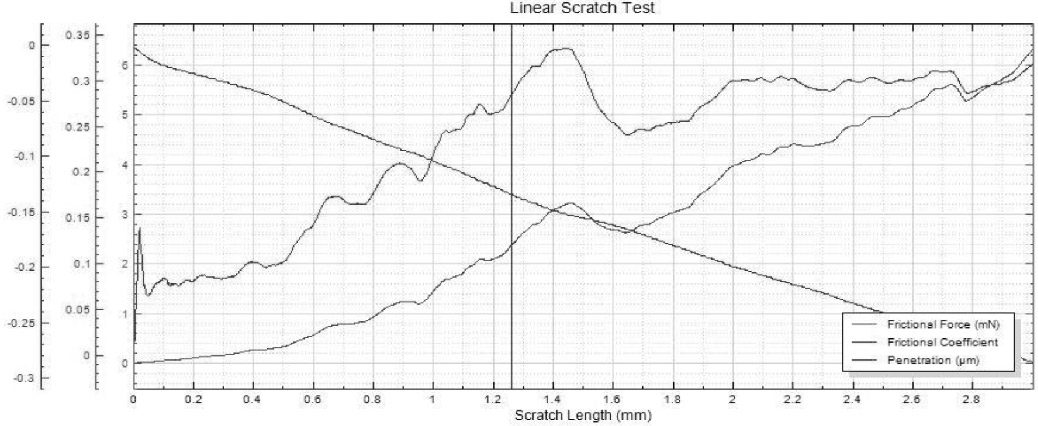
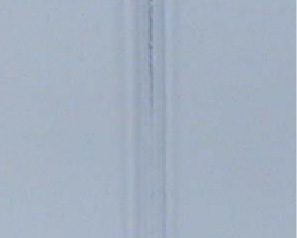
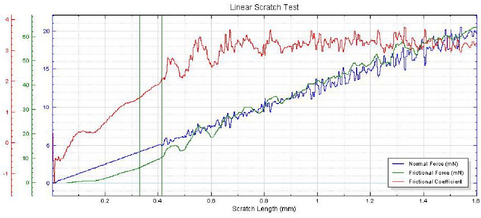
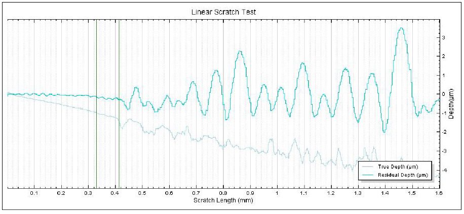
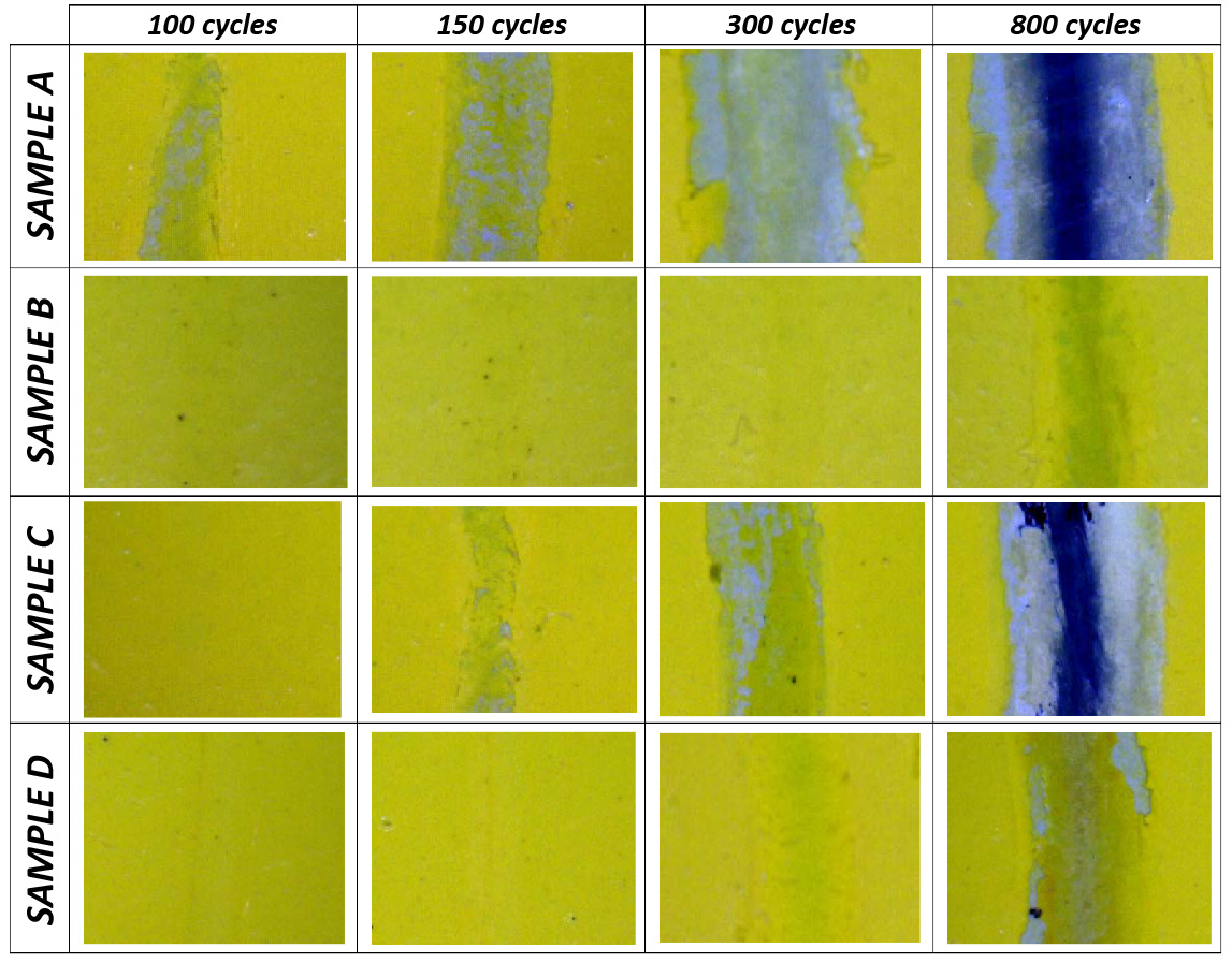
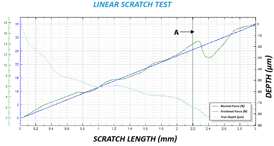
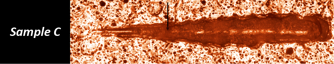
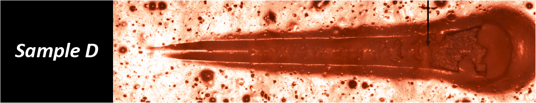
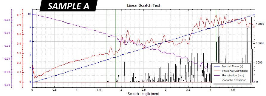
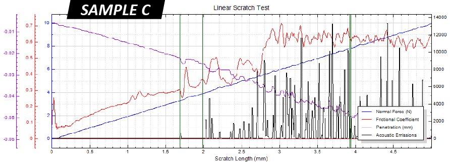
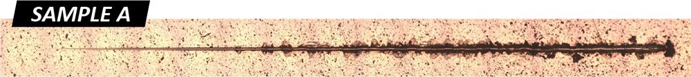
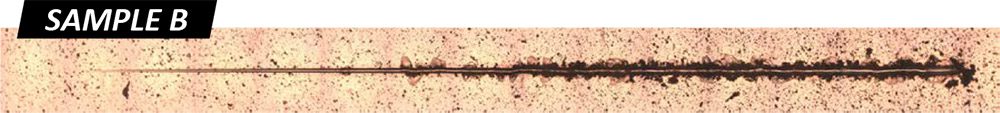
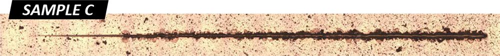
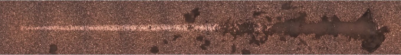
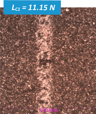
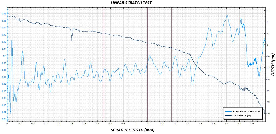
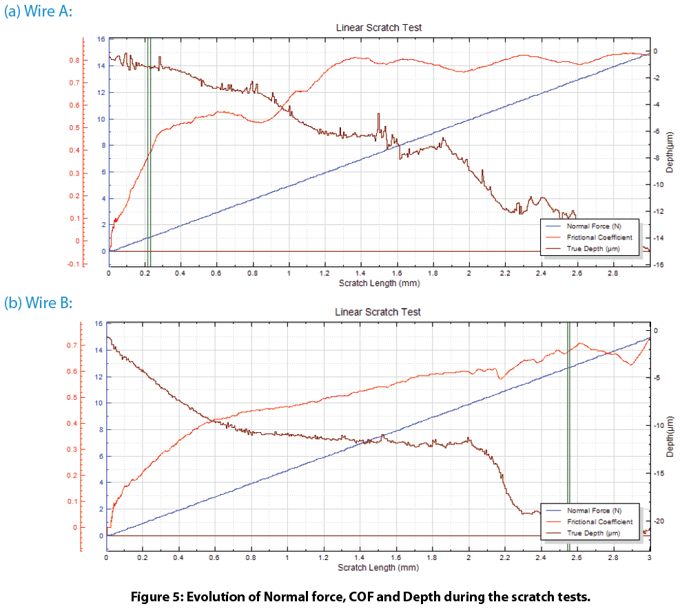
Figure 4 shows the scratch tracks on the wires after testing. The protective layer of Wire A exhibits very good scratch resistance. It delaminates at a load of ~12.6 N. In comparison, the protective layer of Wire B failed at a load of ~1.0 N. Such a significant difference in scratch resistance for these wires contributes to their wear performance, where Wire A possesses substantially enhanced wear resistance. The evolution of normal force, COF, and depth during the scratch tests shown in Fig. 5 provides more insight on coating failure during tests.


Conclusion


In this controlled study we showcased the Nanovea’s tribometer conducting quantitative evaluation of wear resistance for surface treated copper wires and Nanovea’s mechanical tester providing reliable assessment of copper wire scratch resistance. Wire surface treatment plays a critical role in the tribo-mechanical properties during their lifetime. Proper surface treatment on Wire A significantly enhanced wear and scratch resistance, critical in the performance and lifespan of electrical wires in rough environments. Nanovea’s tribometer offers precise and repeatable wear and friction testing using ISO and ASTM compliant rotative and linear modes, with optional high temperature wear, lubrication, and tribo-corrosion modules available in one pre-integrated system. Nanovea’s unmatched range is an ideal solution for determining the full range of tribological properties of thin or thick, soft or hard coatings, films, and substrates.

NOW, LET'S TALK ABOUT YOUR APPLICATION

Understanding Coating Failures using Scratch Testing

Introduction:

Surface engineering of materials plays a significant role in a variety of functional applications, ranging from decorative appearance to protecting the substrates from wear, corrosion and other forms of attacks. An important and overriding factor that determines the quality and service lifetime of the coatings is their cohesive and adhesive strength.

Click here to read!

Scratch Resistance of Cellphone Screen Protectors

Scratch Resistance of Cellphone Screen Protectors

Learn more
 

Importance of Testing Screen Protectors

Although phone screens are designed to resist shattering and scratching, they are still susceptible to damage. Daily phone usage causes them to wear and tear, e.g. accumulate scratches and cracks. Since repairing these screens can be expensive, screen protectors are an affordable damage prevention item commonly purchased and used to increase a screen’s durability.


Using the Nanovea PB1000 Mechanical Tester’s Macro Module in conjunction with the acoustic emissions (AE) sensor, we can clearly identify critical loads at which screen protectors show failure due to scratch1 testing to create a comparative study between two types of screen protectors.


Two common types of screen protector materials are TPU (thermoplastic polyurethane) and tempered glass. Of the two, tempered glass is considered the best as it provides better impact and scratch protection. However, it is also the most expensive. TPU screen protectors on the other hand, are less expensive and a popular choice for consumers who prefer plastic screen protectors. Since screen protectors are designed to absorb scratches and impacts and are usually made of materials with brittle properties, controlled scratch testing paired with in-situ AE detection is an optimal test setup for determining the loads at which cohesive failures (e.g. cracking, chipping and fracture) and/or adhesive failures (e.g. delamination and spallation) occur.


Measurement Objective

In this study, three scratch tests were performed on two different commercial screen protectors using Nanovea’s PB1000 Mechanical Tester’s Macro Module. By using an acoustic emissions sensor and optical microscope, the critical loads at which each screen protector showed failure(s) were identified.


Test Procedure and Procedures

The Nanovea PB1000 Mechanical Tester was used to test two screen protectors applied onto a phone screen and clamped down to a friction sensor table. The test parameters for all scratches are tabulated in Table 1 below.


Results and Discussion

Because the screen protectors were made of a different material, they each exhibited varying types of failures. Only one critical failure was observed for the TPU screen protector whereas the tempered glass screen protector exhibited two. The results for each sample are shown in Table 2 below. Critical load #1 is defined as the load at which the screen protectors started to show signs of cohesive failure under the microscope. Critical load #2 is defined by the first peak change seen in the acoustic emissions graph data.


For the TPU screen protector, Critical load #2 correlates to the location along with the scratch where the protector began to visibly peel off the phone screen. A scratch appeared on the surface of the phone screen once Critical load #2 was surpassed for the remainder of the scratch tests. For the Tempered Glass screen protector, Critical load #1 correlates to the location where radial fractures began to appear. Critical load #2 happens towards the end of the scratch at higher loads. The acoustic emission is a larger magnitude than the TPU screen protector, however, no damage was done to the phone screen. In both cases, Critical load #2 corresponded to a large change in depth, indicating the indenter had pierced through the screen protector.


Conclusion


In this study we showcase the Nanovea PB1000 Mechanical Tester’s ability to perform controlled and repeat-able scratch tests and simultaneously use acoustic emission detection to accurately identify the loads at which adhesive and cohesive failure occur in screen protectors made of TPU and tempered glass. The experimental data presented in this document supports the initial assumption that Tempered Glass performs the best for scratch prevention on phone screens.


The Nanovea Mechanical Tester offers accurate and repeatable indentation, scratch, and wear measurement capabilities using ISO and ASTM compliant Nano and Micro modules. The Mechanical Tester is a complete system, making it the ideal solution for determining the full range of mechanical properties of thin or thick, soft or hard coatings, films, and substrates.

NOW, LET'S TALK ABOUT YOUR APPLICATION

Multi Scratch Automation of Similar Samples using the PB1000 Mechanical Tester

Introduction :

Coatings are widely used in various industries because of their functional properties. A coating’s hardness, erosion resistance, low friction, and high wear resistance are just some of the many properties that make coatings important. A commonly used method to quantify these properties is scratch testing, this allows for a repeatable measurement of a coating’s adhesive and/or cohesive properties. By comparing the critical loads at which failure occurs, the intrinsic properties of a coating can be evaluated.

Click to learn more!

A BETTER Look at Polycarbonate Lens

A BETTER Look at Polycarbonate Lens Learn more
 
Polycarbonate lenses are commonly used in many optical applications. Their high impact resistance, low weight, and cheap cost of high-volume production makes them more practical than traditional glass in various applications [1]. Some of these applications require safety (e.g. safety eyewear), complexity (e.g. Fresnel lens) or durability (e.g. traffic light lens) criteria that are difficult to meet without the use of plastics. Its ability to cheaply meet many requirements while maintaining sufficient optical qualities makes plastic lenses stand out in its field. Polycarbonate lenses also have limitations. The main concern for consumers is the ease at which they can be scratched. To compensate for this, extra processes can be carried out to apply an anti-scratch coating. Nanovea takes a look into some important properties of plastic lens by utilizing our three metrology instruments: Profilometer, Tribometer, and Mechanical Tester.   Click to Read More!

Mechanical Properties of Silicon Carbide Wafer Coatings

Understanding the mechanical properties of silicon carbide wafer coatings is critical. The fabrication process for microelectronic devices can have over 300 different processing steps and can take anywhere from six to eight weeks. During this process, the wafer substrate must be able to withstand the extreme conditions of manufacturing, since a failure at any step would result in the loss of time and money. The testing of hardness, adhesion/scratch resistance and COF/wear rate of the wafer must meet certain requirements in order to survive the conditions imposed during the manufacturing and application process to insure a failure will not occur.

Mechanical Properties of Silicon Carbide Wafer Coatings