Category: Application Notes
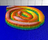
In Situ Morphology at High Temperature Using 3D Profilometry
High temperature environment can change the surface texture, roughness and shapes of materials, resulting in device malfunction and mechanical failures. To ensure the quality of materials or devices used at elevated temperatures, accurate and reliable in situ morphology monitoring of the shape evolution at high temperatures is in need to provide insight into the mechanism of material deformation. Moreover, real-time monitoring of surface morphology at high temperatures is very useful in materials processing, such as laser machining. The Nanovea 3D Non-Contact Profilometers measure the surface morphology of materials without touching the sample, avoiding introducing additional scratches or shape alteration which may be caused by contact technologies such as sliding stylus. Its capacity of non-contact measurement also makes it possible to measure the shape of melted samples.
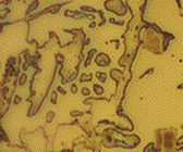
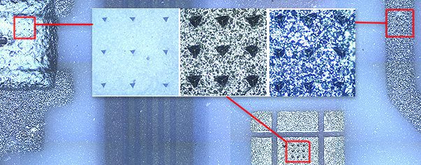
Metallurgy Study of Multiphase Material Using Nanoindentation
Metallurgy studies the physical and chemical behavior of metallic elements, as well as their intermetallic compounds and alloys. Metals undergoing working processes, such as casting, forging, rolling, extrusion and machining, etc., change their phases, microstructure and texture, which results in varied physical properties including hardness, strength, toughness, ductility, and wear resistance. Metallography is often applied to learn the formation mechanism of such specific phases, microstructure and texture.
Metallurgy Study of Multiphase Material Using Nanoindentation
Anodized Aluminum Surface Texture Effect On Luster
Anodizing is an electrolytic passivation process commonly applied to convert aluminum to aluminum oxide. It can modify the surface texture and changes the microstructure of the metal near the surface. Such an anodized aluminum oxide layer is generally much stronger and more adherent than most types of paint and metal plating. It can significantly enhance corrosion and wear resistance and improve cosmetic effects of the products. Anodized aluminum is widely used on electronic devices and consumer products, such as cell phones, cameras, mp3 players and many others.
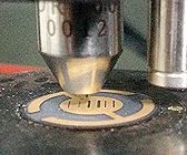
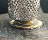
Gold Coating Adhesion on Quartz Crystal Substrate
As an extremely accurate device, the Quartz Crystal Microbalance (QCM) measures the mass change down to 0.1 nanogram. Any mass loss or delamination of the electrodes on the quartz plate will be detected by the quartz crystal and cause significant measurement errors. As a result, the intrinsic quality of the electrode gold coating and the interfacial integrity of the coating/substrate system play an essential role in performing accurate and repeatable mass measurement. The Micro scratch test is a widely used comparative measurement to evaluate the relative cohesion or adhesion properties of coatings based on comparison of the critical loads at which failures appear. It is a superior tool for reliable quality control of QCMs.

Surface Finish of Quartz Crystal Microbalance
Reliable quality control heavily relies upon accurate, quantifiable and reproducible surface inspection. Flatness & finish of the Quartz Crystal Microbalance (QCM) surface are vital to its accuracy and both measurements in 3D guarantees proper manufacture processing and control measures. Unlike a touch probe technique, the Nanovea Profilometer performs a 3D non-contact surface measurement of the sample. This eliminates the risk of creating micro scratches on the QCM surface that may cause inaccuracy or errors in the mass measurement.
Coating Tribology of Gold on Quartz Crystal Substrate
The QCM works based on the piezoelectric properties of the quartz crystal. It measures the mass change on the surface down to 0.1 nanogram during material deposition by detecting variations in the resonance frequency of the crystal. Due to the extreme sensitive and accurate characteristics of the QCM, it is critical to ensure that the two electrodes on both sides of the quartz plate possess good wear resistance. Any mass loss on the metal electrodes caused by wear can lead to significant error in the measurement. Therefore, reliable and accurate wear evaluation using a Tribometer is important for quality control and R&D of QCMs.
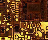
3D Topography With Image Overlay of PCB
The more sophisticated electronic design and layout of semiconductor chips, circuits and systems requires high precision manufacturing and superior quality control. Unlike other techniques such as touch probes or interferometry, the Nanovea 3D Non-Contact Profilometer, using axial chromatism, can measure nearly any material surface. Nano through macro range is obtained during surface profile measurement with zero influence from sample reflectivity, absorption and high surface angles. This is ideal for surface inspection of the PCB assembly (PCBA), which contains a variety of electronic components of different materials, reflectivity and fine features. Moreover, the non-contact profiling technique measures the surface features without touching the PCBA, avoiding the risk of damaging the delicate circuits and electronic components due to sliding of the probe stylus. The combination of high precision, high speed, non-contact and user friendliness makes the Nanovea Profilometer an ideal tool for PCBA inspection.
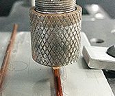
Copper Wire Coating Failure Using Tribology
The surface quality of copper wire is critical in its service performance and lifetime. The micro defects in the wire surface may lead to excessive wear, crack initiation and propagation, and inadequate solderability. Proper surface treatment can remove surface defects that are generated during wire drawing, and improve the corrosion, wear and scratch resistance of the copper wire. Many applications such as aerospace and commercial airliner require copper wires to behave in a controlled manner to prevent unexpected equipment failure. Quantifiable and reliable measurements are in need in order to quantitatively evaluate the wear and scratch resistance of the copper wire surface.
Mechanical Property Broadview Mapping Tool
Seen above is an example of Nanovea’s patent pending Broadview Map Selection Tool. This new tool allows users easy selection of any location on a broad stitched surface view of the sample. Additionally, the user can select all testing parameters at each location, either for a one test or a multi-tests mapping. All locations and test parameters can be saved in easily retrievable recipes. This significant advancement provides fast & friendly Nano through Macro mechanical property studies. Learn more in this months app note: Mechanical Property Mapping
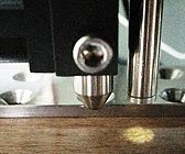
Wood Hardness & Elastic Modulus Using Microindentation
In this application, the Nanovea Mechanical Tester, in microindentation mode is used to compare the mechanical properties of three different types of wood. We would like to showcase the capacity of Nanovea Mechanical Tester in performing hardness and Young’s modulus on wood samples with high precision and reproducibility.