Here are examples of materials we tested this month:
Mechanical:
• Nanoindentation & scratch of thin sapphire coatings
• Nanoindentation of DLC coatings
• Nano scratch of thin teflon coatings
• Microindentation yield strength of micro aluminum parts
• Macro scratch of firearm parts
3D Non-Contact Profilometry:
• Roughness of transparent films
• Texture consistency of laser etch
• Step height of carbon nano tube coatings
• Coplanarity of ball grid arrays
• Medical staples curvature measurement
Tribology:
• Wear rate of wear resistant tooling
• Lubricated linear wear resistance of thin coatings
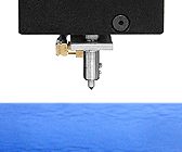
Wear & Friction Of Polymer Belts Using Tribometer
In this study, we simulated and compared the wear behaviors of belts with different surface texture to showcase the capacity of Nanovea Tribometer in simulating the wear process of the belt in a controlled and monitored manner.
DMA Frequency Sweep On Polymer Using Nanoindentation
In this application, the Nanovea Mechanical Tester, in Nanoindentation mode is used to study the
viscoelastic properties of a polished tire sample at different DMA frequencies.
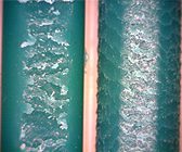
Roughness & Texture Of Polymer Belts Using 3D Profilometry
The roughness and texture of two belts were measured and compared using the Nanovea ST400 optical profilometer to showcase the capability of the Nanovea optical profilometer in providing comprehensive and user friendly surface analysis of belts with different textures.
Here are examples of materials we tested this month:
Mechanical:
• Nanoindentation of individual phases within metal cross section
• Nanoindentation hardness of thin polymer sheeting
• Macro scratch testing of titanium nitride coatings
• Macro scratch testing of Xylan coating
3D Non-Contact Profilometry:
• Roughness of nonwoven fabrics
• Topography of pipe sealant
• Coplanarity measurement of ball grid arrays
• Dimensions of aspheric lenses
Tribology:
• Friction testing of bicycle grease
• High temperature wear testing of ceramic casting material
Here are examples of materials we tested this month:
Mechanical:
• Nanoindentation of thin, hard oxide coatings
• Nanoindentation & scratch of hard titanium nitride coatings
• Microindentation compression of foams
• Microscratch of thin, hard oxide coating
3D Non-Contact Profilometry:
• Roughness & grain size analysis of dental implant
• Roughness of wood flooring finishes
• Roughness of building drywall
• Coplanarity of pin grid array under elevated temperature
Tribology:
• Wear testing of cryogenically hardened steel
• Friction testing doggie treats
• Tribocorrosion of dlc coatings
Profilometer For Large Area Measurements
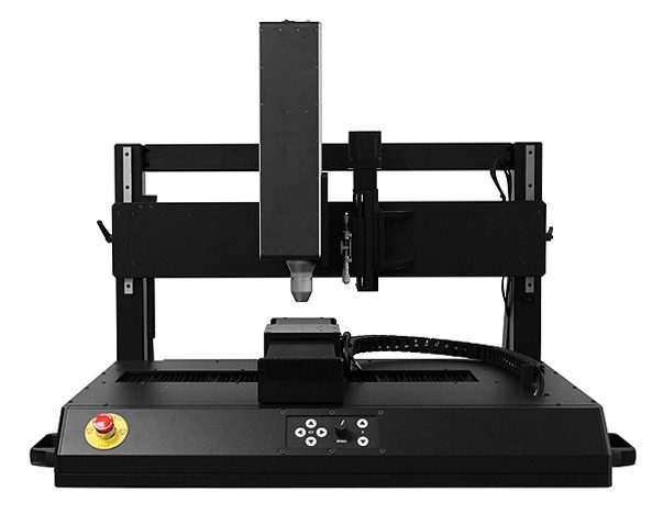
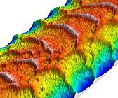
Meet the ST500 Profilometer. After years of success with the ST400 and HS1000 Nanovea introduces the ST500 providing high speed large area measurement without stitching. The ST500 has a 400 mm X-Y Axis Travel, a 50 mm Z Axis with a maximum speed up to 200 mm/s. The system can be equipped with either an optical pen or line scanner for ultra fast measurement (384,000 points per second). Unlike other technologies, each point is a direct, full depth of field during large area measurement without the need of refocusing. A video zoom camera can also be used to provide automatic function to large area measurement complete on a desktop user friendly platform. See app note for example.
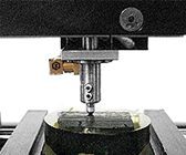
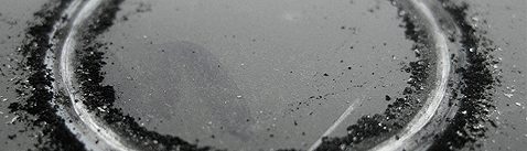
Scratch Adhesion Testing of Disc Coatings
In this study, instrumented scratch testing is used to assess the failure modes of the top layers of CD and BD. This test allows users to quantitatively compare the scratch resistance of different protective coatings.
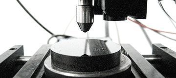
Wear Evaluation by High Load Tribometer
The Macro Tribometer is designed with high torque capability for loads up to 500 N. In this study, we simulated and compared the wear behaviors of valve coatings under high loads to showcase the capacity of Nanovea Macro Tribom
eter in quantitatively evaluating the wear properties of materials such as wear rate and coefficient of friction.
Here are examples of materials we tested this month:
Mechanical:
• Nanoindentation & Scratch of blank coins
• Nanoindentation of electroplated coating
• Nanoindetation dma of epoxy adhesive coating
3D Non-Contact Profilometry:
• Roughness of tablet press punch
• Step height of titanium oxide films
• Dimensions of metal chamfered edge
Tribology:
• Wear testing of enriched teflon
• Wear testing of nylon composite