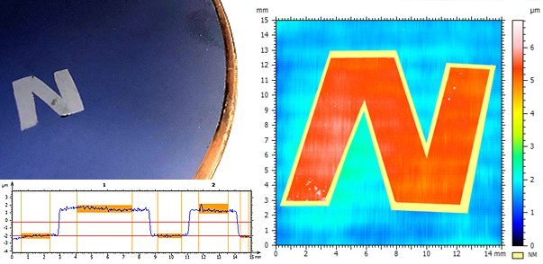
Wafer Coating Thickness Measurement Using 3D Profilometry
Wafer Coating Thickness Measurement is critical. Silicon wafers are widely used in the making of integrated circuits and other micro devices used in a vast number of industries. A constant demand for thinner and smoother wafers and wafer coatings makes the Nanovea 3D non-contact Profilometer a great tool to quantify coating thickness and roughness of just about any surface. The measurements in this article were taken from a coated wafer sample in order to demonstrate the capabilities of our 3D Non-Contact Profilometer.


