Category: Profilometry Testing
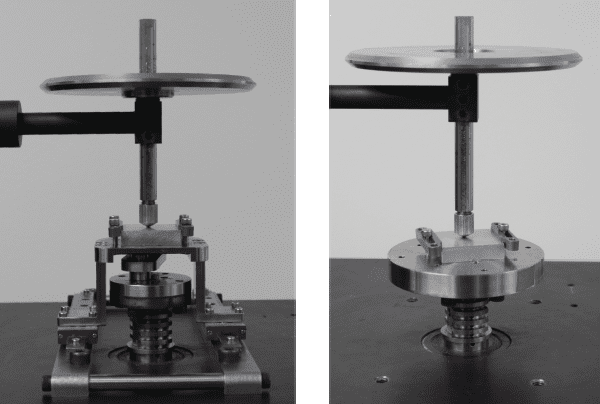
Rotative or Linear Wear & COF? (A Comprehensive Study Using the Nanovea Tribometer)
Wear is the process of removal and deformation of material on a surface as a result of the mechanical action of the opposite surface. It is influenced by a variety of factors, including unidirectional sliding, rolling, speed, temperature, and many others. The study of wear, tribology, spans many disciplines, from physics and chemistry to mechanical engineering and material science. The complex nature of wear requires isolated studies toward specific wear mechanisms or processes, such as adhesive wear, abrasive wear, surface fatigue, fretting wear, and erosive wear. However, “Industrial Wear” commonly involves multiple wear mechanisms occurring in synergy.
Linear reciprocating and Rotative (Pin on Disk) wear tests are two widely used ASTM-compliant setups for measuring sliding wear behaviors of materials. Since the wear rate value of any wear test method is often used to predict the relative ranking of material combinations, it is extremely important to confirm the repeatability of the wear rate measured using different test setups. This enables users to carefully consider the wear rate value reported in the literature, which is critical in understanding the tribological characteristics of materials.
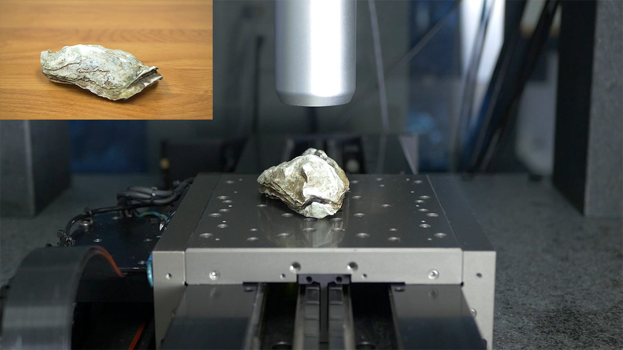
High Speed Characterization of an Oyster Shell
Large samples with complex geometries can prove difficult to work with due to sample preparation, size, sharp angles, and curvature. In this study an oyster shell will be scanned to demonstrate the Nanovea HS2000 Line Sensor’s capability to scan a large, biological sample with complex geometry. While a biological sample was used in this study, the same concepts can be applied to other samples.


Surface Finish Inspection of Wood Flooring
Importance of Profiling Wood Finishes
In various industries, the purpose of a wood finish is to protect the wooden surface from various types of damage such as chemical, mechanical or biological and/or provide a specific visual aesthetic. For manufacturers and buyers alike, quantifying surface characteristics of their wood finishes can be vital to the quality control or optimization of finishing processes for wood. In this application, we will explore the various surface features that can be quantified using a Nanovea 3D Non-Contact Profilometer.
Quantifying the amount of roughness and texture that exists on a wooden surface can be essential to know in order to ensure it can meet the requirements of its application. Refining the finishing process or checking the quality of wooden surfaces based on a quantifiable, repeatable and reliable surface inspection method would allow manufacturers to create controlled surface treatments and buyers the ability to inspect and select wood materials to meet their needs.
Measurement Objective
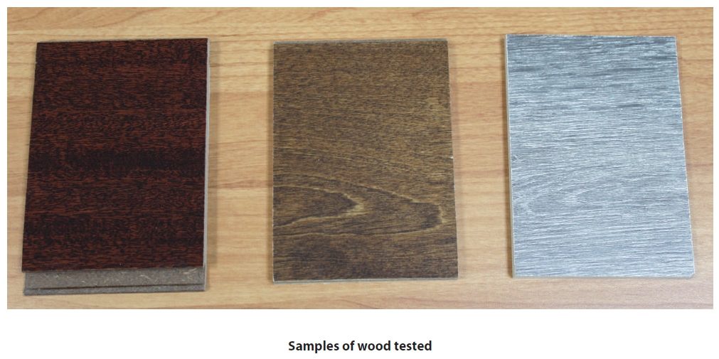
In this study, the high-speed Nanovea HS2000 profilometer equipped with a non-contact profiling line sensor was used to measure and compare the surface finish of three flooring samples: Antique Birch Hardwood, Courtship Grey Oak, and Santos Mahogany flooring. We showcase the capability of the Nanovea Non-Con-tact Profilometer in delivering both speed and precision when measuring three types of surface areas and a comprehensive in-depth analysis of the scans.
Test Procedure and Procedures
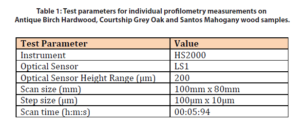
Results and Discussion
Sample description: Courtship Grey Oak and Santos Mahogany flooring are laminate flooring types. Courtship Grey Oak is a low gloss, textured slate gray sample with an EIR finish. Santos Mahogany is a high gloss, dark burgundy sample that was prefinished. Antique Birch Hardwood has a 7-layer aluminum oxide finish, providing everyday wear and tear protection.
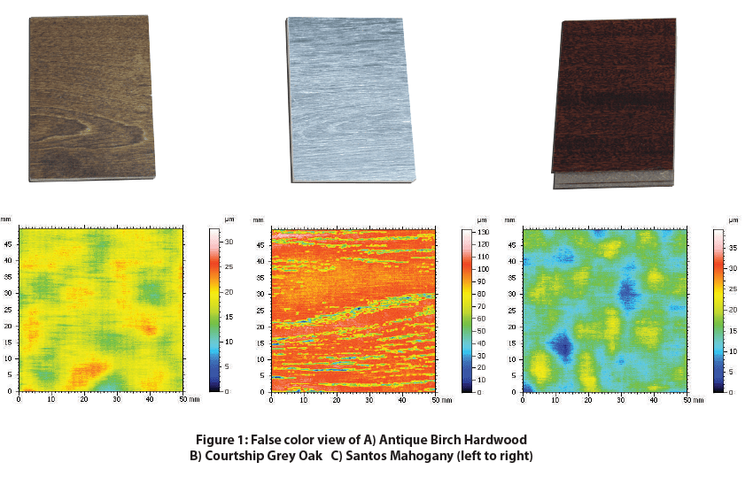
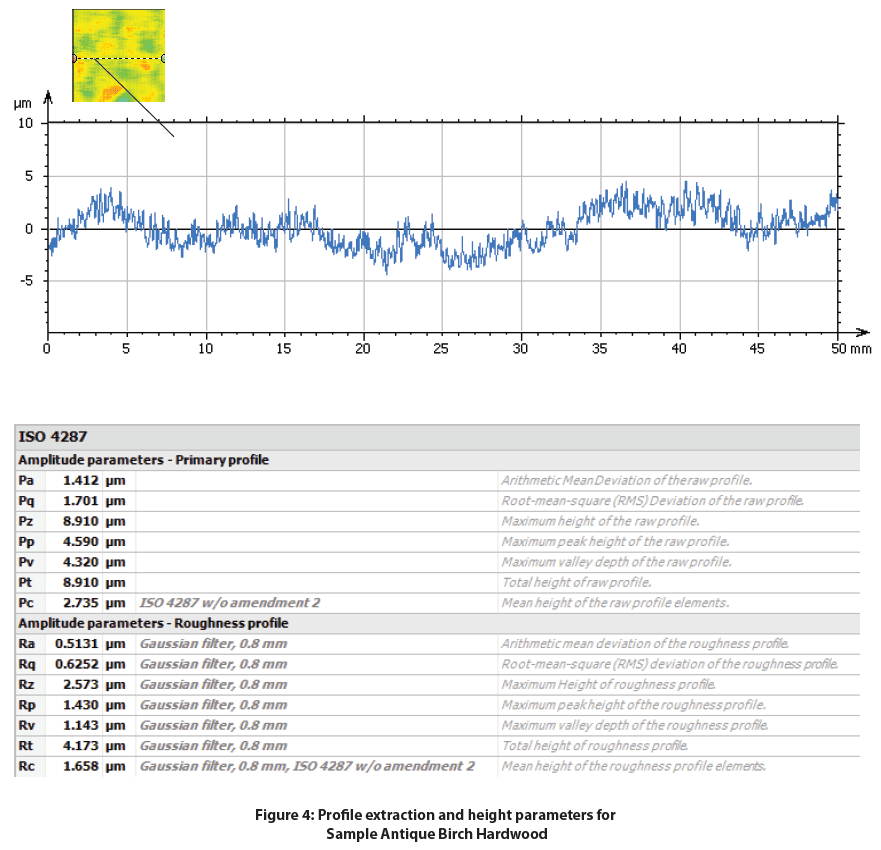
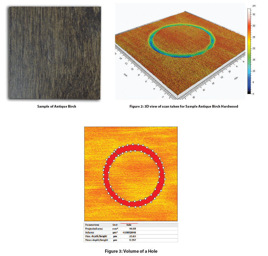
Antique Birch Hardwood
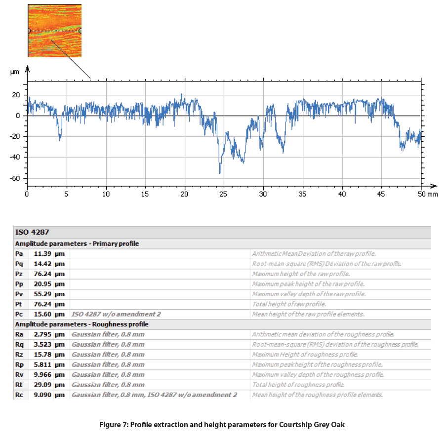
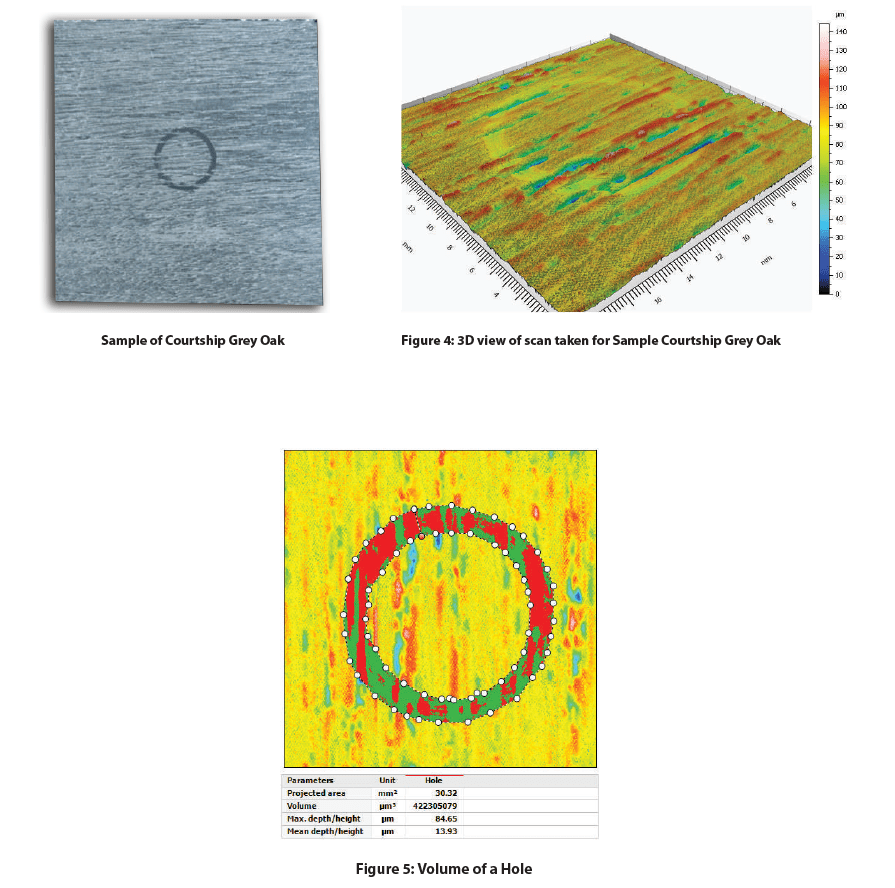
Courtship Grey Oak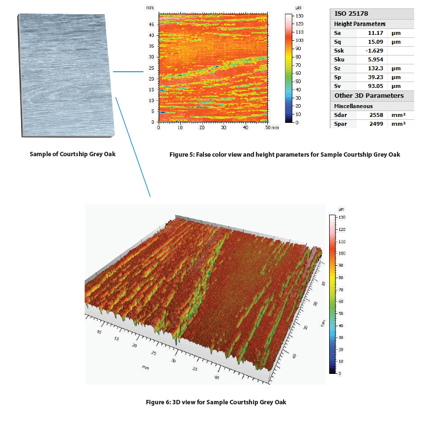
Santos Mahogany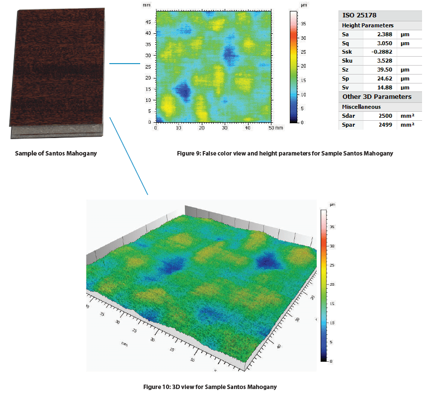

Discussion
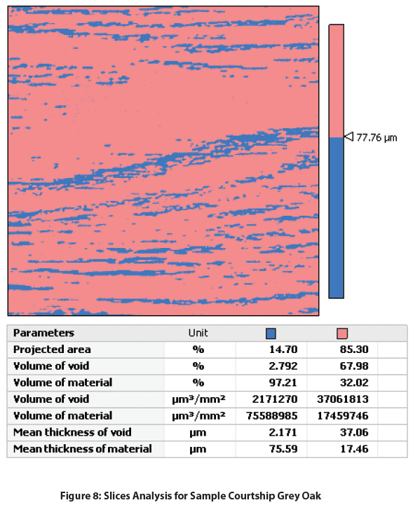
There is a clear distinction between all the samples’ Sa value. The smoothest was Antique Birch Hardwood with a Sa of 1.716 µm, followed by Santos Mahogany with a Sa of 2.388 µm, and significantly increasing for Courtship Grey Oak with a Sa of 11.17 µm. P-values and R-values are also common roughness values that can be used to assess the roughness of specific profiles along the surface. The Courtship Grey Oak possess-es a coarse texture full of crack-like features along the wood’s cellular and fiber direction. Additional analysis was done on the Courtship Grey Oak sample because of its textured surface. On the Courtship Grey Oak sample, slices were used to separate and calculate the depth and volume of the cracks from the flatter uniform surface.
Conclusion

In this application, we have shown how the Nanovea HS2000 high-speed profilometer can be used to inspect the surface finish of wood samples effectively and efficiently. Surface finish measurements can prove to be important to both manufactures and consumers of hardwood flooring in understanding how they can improve a manufacturing process or choose the appropriate product that performs best for a specific application.

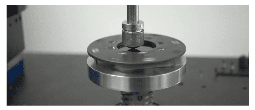
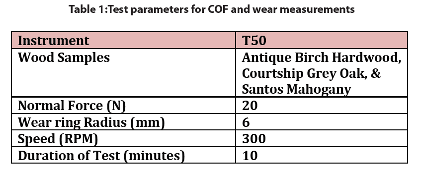
Wood Wear Test with the Nanovea Tribometer
Importance of Comparing Wood Finish Wear & COF
Wood has been used for thousands of years as a building material for homes, furniture, and flooring. It has a combination of natural beauty, and durability, making it an ideal candidate for flooring. Unlike carpet, hardwood floors keep their color for a long time and can be easily cleaned and maintained, however, being a natural material, most wood flooring requires the application of a surface finish to protect the wood from various kinds of damage such as scuffing and chipping over time. In this study, a Nanovea Tribometer was used to measure the wear rate and coefficient of friction (COF) to better understand the comparative performance of three wood finishes.
The service behavior of a wood species used for flooring is often related to its wear resistance. The change in the individual cellular and fiber structure of different species of wood contributes to their different mechanical and tribological behaviors. Actual service tests of wood as flooring materials are expensive, difficult to duplicate, and require long periods of testing time. As a result, it becomes valuable to develop a simple wear test that can produce reliable, reproducible, and straight forward.
Measurement Objective
In this study, we simulated and compared the wear behaviors of three types of wood to showcase the capability of the Nanovea Tribometer in evaluating the tribological properties of wood in a controlled and monitored manner.
Discussion
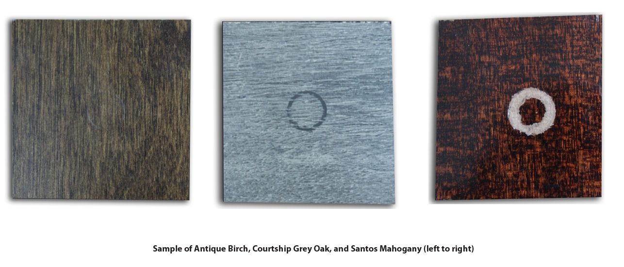
Sample Description: Antique Birch Hardwood has a 7-layer aluminum oxide finish, providing everyday wear and tear protection. Courtship Grey Oak, & Santos Mahogany are both laminate flooring types that vary in surface finish and gloss. The Courtship Grey Oak is a slate gray color, EIR finish, and low gloss. On the other hand, Santos Mahogany is a dark burgundy color, prefinished, and high gloss which allows surface scratches and defects to be more easily hidden.
The evolution of COF during the wear tests of the three wood flooring samples are plotted in Fig. 1. The Antique Birch Hardwood, Courtship Grey Oak, & Santos Mahogany samples all showed different COF behavior.
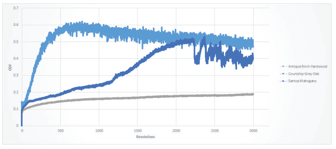
It can be observed in the graph above that Antique Birch Hardwood was the only sample that demonstrated a steady COF for the duration of an entire test. The Courtship Grey Oak’s sharp increase in COF and then gradual decrease could be indicative that the sample’s surface roughness largely contributed to its COF behavior. As the sample wore, the surface roughness decreased and became more homogenous which explains the decrease in COF as the sample surface became smoother from mechanical wear. The COF on Santos Mahogany displays a smooth gradual increase in COF at the beginning of the test and then transitioned abruptly into a choppy COF trend. This could indicate that once the laminate coating started to wear through, the steel ball (counter material) made contact with the wood substrate which wore in a quicker and turbulent manner creating the noisier COF behavior towards the end of the test.
Antique Birch Hardwood:
Courtship Grey Oak:
Santos Mahogany
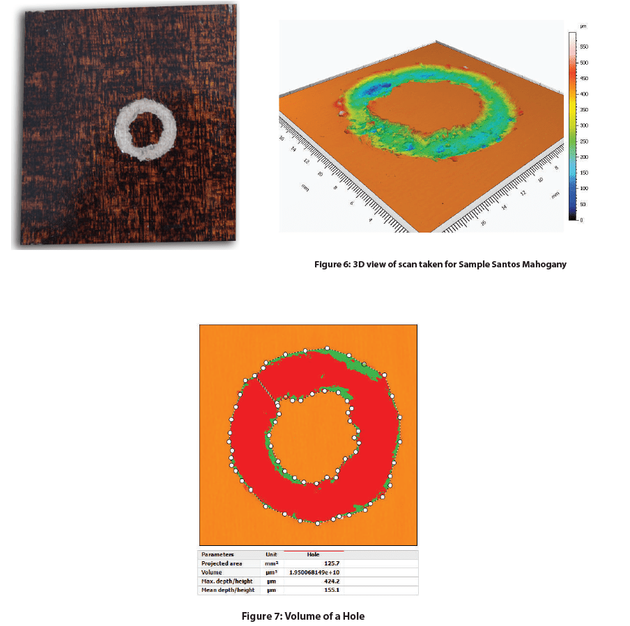
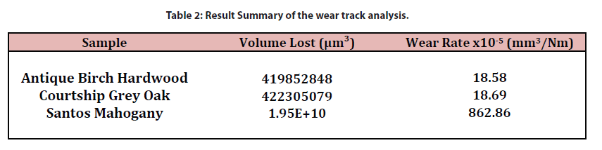
Table 2 summarizes the results of the wear track scans and analysis on all wood flooring samples after the wear tests were performed. Detailed information and images for each sample can be seen in Figures 2-7. Based on the Wear Rate comparison between all three samples, we can deduct that Santos Mahogany proved to be less resilient to mechanical wear than the other two samples. Antique Birch Hardwood and Courtship Grey Oak had very similar wear rates although their wear behavior during their tests differed significantly. Antique Birch Hardwood had a gradual and more uniform wear trend while Court-ship Grey Oak showed a shallow and pitted wear track due to the pre-existing surface texture and finish
Conclusion

In this study, we showcased the capacity of Nanovea’s Tribometer in evaluating the coefficient of friction and wear resistance of three types of wood, Antique Birch Hardwood, Courtship Grey Oak, and Santos Mahogany in a controlled and monitored manner. The superior mechanical properties of the Antique Birch Hardwood leads to its better wear resistance. The texture and homogeneity of the wood surface play an important role in the wear behavior. The Courtship Grey Oak surface texture such as gaps or cracks between the wood cell fibers may become the weak spots where the wear initiates and propagates.
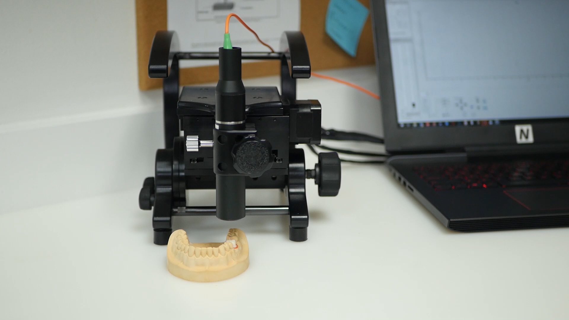
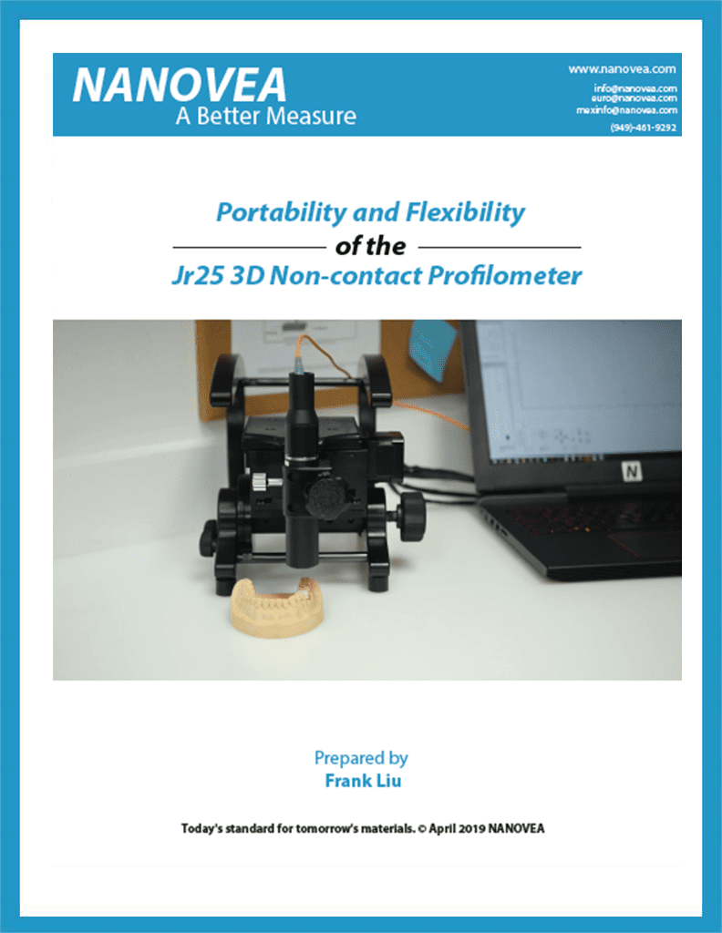
Portability and Flexibility of the Jr25 3D Non-contact Profilometer
Understanding and quantifying a sample’s surface is crucial for many applications including quality control and research. To study surfaces, profilometers are often used to scan and image samples. A large problem with conventional profilometry instruments is the inability to accommodate for non conventional samples. Difficulties in measuring non conventional samples can occur due to sample size, geometry, inability to move the sample, or other inconvenient sample preparations. Nanovea’s portable 3D non-contact profilometers, the JR series, is able to solve most of these problems with its ability to scan sample surfaces from varying angles and its portability.
Read about the Jr25 Non-contact Profilometer!
Quality Analysis on Electrical Discharge Machined Metals
Electrical discharge machining, or EDM, is a manufacturing process that removes material via electrical
discharges [1]. This machining process is generally used with conductive metals that would be difficult
to machine with conventional methods.
As with all machining processes, precision and accuracy must be high in order to meet acceptable
tolerance levels. In this application note, the quality of the machined metals will be assessed with a
Nanovea 3D non-contact profilometer.


A Better Look at Paper
Paper has played a large role in information distribution since its invention in the 2nd century [1]. Paper consists of intertwined fibers, typically obtained from trees, that have been dried into thin sheets. As a medium for information storage, paper has allowed the spread of ideas, art, and history over long distances and through passing time.
Today, paper is commonly used for currency, books, toiletries, packaging, and more. Paper is processed in different ways to obtain properties to match their application. For example, the visually appealing, glossy paper from a magazine is different compared to rough, cold-pressed watercolor paper. The method in which paper is produced will affect the surface properties of the paper. This influences how ink (or other medium) will settle onto and appear on the paper. To inspect how different paper processes affect surface properties, Nanovea inspected the roughness and texture of various types of paper by conducting a large area scan with our 3D Non-Contact Profilometer.
Click to learn about the Surface Roughness of Paper!


A BETTER Look at Polycarbonate Lens


500nm Glass Step Height: Extreme Accuracy with Non-Contact Profilometry
Surface characterization are current topics undergoing intense study. The surfaces of materials are important since they are the regions where physical and chemical interactions between the material and environment occur. Thus, being able to image the surface with high resolution has been desirable, since it allows scientists to visually observe the smallest surface details. Common surface imaging data includes topography, roughness, lateral dimensions, and vertical dimensions. Identifying the load bearing surface, spacing and step height of fabricated microstructures, and defects on the surface are some applications that can be obtained from surface imaging. All surface imaging techniques, however, are not created equal.
500nm Glass Step Height: Extreme Accuracy with Non-Contact Profilometry
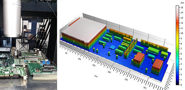
Automated Large Area Profilometry of PCB
Scaling up of manufacturing processes is necessary for industries to grow and keep up with constantly increasing demands. As manufacturing process scales up, the tools used in quality control also need to be scaled up. These tools must be fast to keep up with the production rate, while still maintaining high accuracy to meet product tolerance limits. Here, the Nanovea HS2000 Profilometer, with Line Sensor, showcases its value as a quality control instrument with its fast, automated, and high-resolution large area profilometry capabilities.
Video Clip or App Note: Automated Large Area Profilometry of PCB