Category: Application Notes
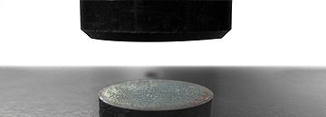
Surface Area Measurement of Oxidation With 3D Profilometry
The 3D Non Contact Profilometer will be used to characterize the surface area measurement of two samples with A1SiN coatings, one with a low level of silicon the other with a high level. The A1SiN coating was deposited on H13 Steel by magnetron sputtering then submitted to an oxidation resistance test (900°C-1hour).

Tribological Characterization of Ti-WS2 Coating
In this report we will review the tribological characterization of Ti-WS2 coating deposited by Magnetron Sputtering technique. The friction and wear tribology will be obtained with the Tribometer in reciprocating mode and an integrated optical profiler will be used to obtain wear rate.
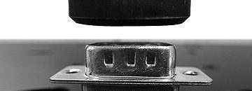
Scratch Resistance of Microstructure using Scratch Testing
In this application, the Nanovea Mechanical Tester in its nano scratch testing mode is used to measure the load required to cause failure to a microstructure. We must simulate the process of scratching in a controlled and monitored manner to observe scratch resistance. A 10μm diamond tipped stylus is used at a progressive load ranging from 10 mN to 20 mN to scratch the microstructure. The point where the coating fails by cracking is taken as the point of failure.
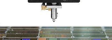
Connector Pin Inspection With 3D Profilometry
In this application, the Nanovea ST400 Profilometer is used to measure the full area of a connector surface and its pins. The application was chosen for its challenging features while highlighting the measurement options with Nanovea’s technique. There is an endless list surface parameters that can be automatically calculated after the surface scan. Here we will review a full 3D profile, flatness of the connector base, coplanarity of the pins and the roughness of a pin tip.