Mechanical Characterization of Organic & Non Organic Shell
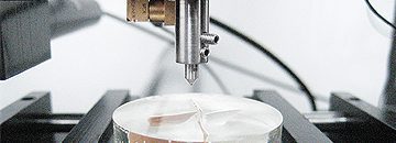
In this application, the Nanovea Mechanical Tester, in Nanoindentation mode, is used to study the mechanical characterization of an organic and a non-organic egg shell. The most critical aspect with Nanoidentation testing is securing the sample, here we took pieces of each sample and epoxy mounted leaving the edges exposed for testing.
Here are examples of materials we tested this month:
Mechanical:
• Nanoindentation of xylan coating
• Nanoindentation composite
• Nanoindentation mapping of wood
• Nanofriction of catheter
• Nano Scratch of silicon
• Micro Scratch of silicon nitride coating
3D Non-Contact Profilometry:
• Topography of corroded steel
• Dimension of optical lens samples
• Roughness of polymer molds
• Roughness of polymer casing
• Depth of pitted aluminum
• Step height micro features
• Friction Testing of various lubricants
• Xylan coatings wear resistance
• Wear rate (high speed) of hard plastic
R&D MAGAZINE RECOGNIZING NANOVEA M3
The control loop between the piezo-electric transducer in the Nanovea M3, combined with an ultra sensitive load cell, helps ensure that the load applied is accurate and reproducible. High precision of the capacitive ring enables accurate depth measurement providing an automatic depth versus load curve with hardness and elastic modulus data meeting ASTM E2546 Nanoindentation requirements using precise motorized staging, the test is repeated quickly to deliver repeatable and accurate averaging of five tests. The Nano Module head also eliminates many of the color and texture problems associated with image recognition software. Read More R&D Magazine
Nanovea Unveils Its New Revolutionary N3 Line
Irvine CA, January 18, 2012 – Nanovea today announced the arrival of the N3 line dedicated to providing high-end measurement technology to the broader market. Nanovea has fully automated their measurement techniques while designing to price in the $20K market.
The headline of the N3 line is the M3, a breakthrough in technology that aims at two distinct aspects missing in the hardness testing market. First, the combination of three factors never before available: nanometer range, controlled load & depth and a competitive price to compete in the $20K market. This provides universities and smaller R&D units to affordable nanoindentation capability. The M3 introduces an entirely new user capability with this price range, providing affordable access too quick and easy nanoindentation results under ASTM standard. Second, is to offer next generation technology to replace the traditional Visual Micro Vickers Hardness Testers that have not changed in more than 15 years. To achieve this, the indentation method has been made fully automated with no need to visually observe the indent which eliminates user error or problems with image recognition software that may have issues with material color and texture. Also, this new technology can achieve lower load and will work on thin coatings and all ranges of materials including ceramics, polymers, metals and others. The fully automated system has a touch screen start that gives automatic average of multiple measurements in minutes. The unit is compact and fully contained with only one standard electrical cable to connect. Because of these advancements in technology and the very competitive price, the M3 line will be the replacement of choice for older Micro Vickers Tester currently used in industrial high throughput quality control environments.
The M3 ushers in a new era of hardness testing by providing measurement capability that until this point targeted very specifically high end research. Essentially, like most technological advancements, price has kept nanoindentation capability out of the reach of the broader market still using standard hardness testing equipment. The M3 will be a significant replacement at an affordable cost and the result will be revolutionary. But Nanovea didn’t stop there. The M3 is only one of three new products from Nanovea’s new N3 line. Along with the M3 Nanovea also introduces the P3 and the T3.
The P3 is a significant advancement with 3D non contact metrology, providing automatic nanometer ISO roughness and step data on nearly any material; a capability unavailable in the 20k market. The P3 will provide to a broader market in need of automatic nano through macro roughness data without the high cost associated with a complete Profilometer system. And last but not least, the T3, like the P3 was developed to provide quick, easy and affordable access to high end measurement capability. The T3 is an automatic nano wear tester using linear reciprocating, ASTM g133, for wear rate study.
“The N3 line is a revolution of high end material measurement instruments, each in their own way and in their own markets. Each has been strategically designed to follow Nanovea’s goal to provide crucial nanotechnology to the broader market. As with many technologies being developed today to advance our society, price will ultimately control broad acceptance and use. It is no different with measurement technology and is just as crucial if not more.” said Pierre Leroux, Nanovea’s CEO.
Nanovea will be releasing the N3 line for the first time publicly at the Fall 2012 MRS show. Purchase orders for the N3 line begin in April for delivery in June 2012.
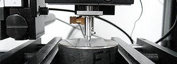
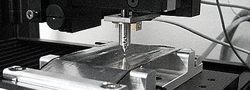
Fracture Resistance of Silicon With Nano Scratch Testing
In this application, the Nanovea Mechanical Tester, in nano scratch testing mode, is used to measure the fracture resistance of a 170μm thick silicon sample. We must simulate the process of scratching in a controlled and monitored manner to observe sample behavior effects. A 2μm diamond tipped stylus is used at a progressive load ranging from 0.5 mN to 400 mN to scratch the silicon surface. Points of failure will be reviewed.
Here are examples of materials we tested this month:
Mechanical:
• Nanoindentation of solar cells
• Nanoindentation puncture of foil
• Nanoindentation yield strength of silicon
• Nanoindentation yield strength of composite
• Nano Scratch of micro features
• Nano Wear of medical coating
• Microindentation yield strength of alloy
3D Non-Contact Profilometry:
• Topography of bug splatter
• Dimension of precision machined part
• Roughness of machined metal samples
• Roughness measurement of medical tubing finish
• Form of micro part
• Warpage of copper samples
Tribology:
• Friction testing of stainless steel
• Friction testing of polymer medical tube
• Wear resistance of ceramic
• Wear rate of glass
• Wear rate of polished graphite
THE MEASUREMENT OF TRUTH. INTERFEROMETRY DISADVANTAGES
Some thoughts on what to consider when reviewing the two white light profilometer techniques. White Light Interferometry disadvantages start with using software and mathematical equations to detect, through the imaging system, the movement of fringes across the screen as the sample or the measuring head is moved up or down in specific steps. These measurements are only as as good as what the software and imaging parts can do in terms of “detecting” the movement of these fringes. When dealing with reflective and smooth surfaces, the accuracy of the data is superior. This is why the technique has been primarily developed for semiconductor applications where surfaces are often reflective and steps, if present, are close to 90° angles.
However, with a rough and low reflective surface, the software interpretation of the real surface becomes far from the truth because of inherent artifacts of the Interferometry technique. In addition to this, Interferometry is also extremely limited in terms of angle measurement. Again, software can now accomplish miracles to complete surfaces with additional information such as expected shape of surface. Previewing the raw data is one way to know what the software has manipulated but even the primary analysis software automatically renders an interpretation of what the surface must look like and automatically completes unmeasured points without the user knowing. With clever software, artifacts can be impossible to distinguish from real data since the rendering of the 3D image will look perfect and often users do not know what their surface really look like. This is especially true when dealing with more complex and difficult surfaces.
Also, speed is brought up as a major difference between the two techniques. It is true that Interferometry can more quickly measure one field of view image to evaluate roughness and step. These are clear advantages when dealing with smooth semiconductor surfaces. But again, if the surface being measured is not smooth the data may be provided more quickly but is far from true data. Additionally, stitching of surfaces works when, again, the surface is smooth and reflective and with clear position markers. The accuracy of stitching will reduce as the surface becomes rougher and with more difficult types of materials. It can become difficult to detect artifacts and issues with this when the surface is rougher than when you see a clear step. To obtain the best lateral resolution is it necessary to use a 100x objective, which limits the measurement area to approximately 140micrometer x 110 micrometer. The number of images to stitch can become a problem when trying to get accurate data on larger parts (100 images for 1mmx1mm and 10000 images for a 10mmx10mm). The lateral resolution of the image is a function of the number of pixels in the camera being used.
Unlike the manipulative Interferometry technique, White light Axial Chromatism technology measures height directly from the detection of the wavelength that hits the surface of the sample in focus. It is direct measurement with no mathematical software manipulation. This provides unmatched accuracy on the surface measured because a data point is either measured accurately without software interpretation or not at all. The software can complete the unmeasured point but the user is fully aware of it and can have confidence that there is no other hidden artifacts. The technique can also measure nearly any material surface with much higher angles up to over 80° in some cases. Axial Chromatism can scan on a length of over 30cm in less than 0.3 second. New acquisition system are now available to reach 31,000 points per second with 1m/s scanning. New line sensors with Axial Chromatism can actually measure up to 324,000points per second. A typical image acquired by an interferometer would have less than 1,000,000 data points per field of view. Using an Axial Chromatism line sensor scanning will take a few seconds which means that the actual speed is very close to Interferometry speeds while providing truer data. Therefore speed should be considered based on the application itself.
The growth of Interferometry technique was mostly due to their success in industries with deeper pockets. Therefore, the cost of Interferometry is generally twice that of Axial Chromatism systems with similar resolution and broader capability. It is our experience that 90% of applications are better served using the Axial Chromatism technique. Clients that have chosen Axial Chromatism technology have rarely been disappointed while there are many pitfalls with the choice of Interferometry. And the regret is almost always the same: Interferometry’s disadvantage of broad measurement capability and reliably true data with a high price tag.
Nano Puncture Resistance Using Nanoindentation
In this application, the Nanovea Mechanical Tester, in Nanoindentation mode is used to study the puncture resistance of an aluminum foil sample using a cylindrical flat tip indenter. A custom sample holder was designed to secure thin film and foil samples.
Here are examples of materials we tested this month:
Mechanical:
• Nanoindentation of sicn coatings
• Nanoindentation stress-strain of polymer
• Nanoindentation yield strength of mems
• Nano Scratch of catheter coatings
• Nano Friction of rtil film
• Micro Scratch of tablet coatings
• Micro Wear of micro copper wire
3D Non-Contact Profilometry:
• Topography of fractured automotive part
• Dimension of ceramic micro features
• Roughness of pvc samples
• Roughness of plastic injection mold
• Flatness of glass samples
• Volume loss of wear tracks
Tribology:
• COF of various oil formulas
• COF of polymer medical tube
• Wear rate of rubber seal
• Wear rate of coil coatings
• Wear rate of carbon coated steel
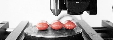
Tablet Coating Failure With Micro Scratch Testing
In this application, the Nanovea Mechanical Tester, in its micro scratch mode, is used to measure the load required to cause the failure to a generic and brand tablet coating. We must simulate the process of scratching in a controlled and monitored manner to observe sample behavior effects. A 20μm diamond tipped stylus is used at a progressive load ranging from 4 N to 8 N to scratch the tablet coating. The point where the coating fails by cracking is taken as the point of failure. Hardness and elastic modulus will also be evaluated in nanoindentation mode.