Monthly Archives: September 2013
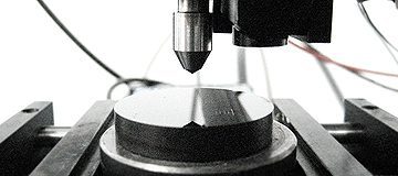
Coating Failure Analysis Using Micro Scratch Testing
We must simulate the process of scratch testing in a controlled and monitored manner to observe coating failure analysis. In this application, the Nanovea Mechanical Tester, in its micro scratch mode, is used to measure the load required to cause the coating failure to three separately processed DLC coatings. A 90° Cone, 20μm diamond tipped stylus is used at a progressive load ranging from 0.01 mN to 15 N to scratch the DLC coating. The point where the coating fails by cracking is taken as the point of failure.
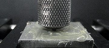
Mechanical Stability of Grease Using Tribometer
The Nanovea Pin-On-Disk Tribometer will be used in rotative mode, linear could have also been used. A steel ball tip will be used against a steel sample coated with lithium complex grease. The load used will be at 5N with a constant speed of 150rpm. Two separately formulated lithium complex greases will be tested for comparative evaluation.
Here are examples of materials we tested this month:
Mechanical:
• Nanoindentation stress strain of steels
• Nanoindentation yield strength of micro parts
• Nanoindentation stiffness of polymers
• Nano Scratch of optical coating
• Micro Scratch of paint coatings
• Macroindentation of dlc coatings
• Macro Scratch of dlc coatings
3D Non-Contact Profilometry:
• Topography of gel surfaces
• Roughness of injection molds
• Texture of silicone samples
• Flatness & Co-Planarity of wafer arrays
• Step Height of photomask
• Dimensions of micro parts
• Submerged Wear Testing of dlc coatings
• Wear Testing silicon coatings
• Friction Testing smart glass samples
Flatness Measurement of Wafer Using 3D Profilometry
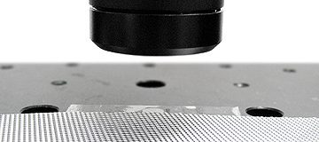
In this application the Nanovea ST400 Profilometer is used to measure the section of a wafer array. The area measured was selected at random, and assumed large enough in that it could be extrapolated to make assumptions about a much larger surface. Surface flatness measurement, planarity & other surface parameters are used to analyze the surface.
