Blog Archives
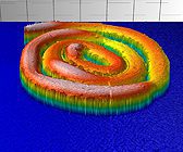
In Situ Morphology at High Temperature Using 3D Profilometry
High temperature environment can change the surface texture, roughness and shapes of materials, resulting in device malfunction and mechanical failures. To ensure the quality of materials or devices used at elevated temperatures, accurate and reliable in situ morphology monitoring of the shape evolution at high temperatures is in need to provide insight into the mechanism of material deformation. Moreover, real-time monitoring of surface morphology at high temperatures is very useful in materials processing, such as laser machining. The Nanovea 3D Non-Contact Profilometers measure the surface morphology of materials without touching the sample, avoiding introducing additional scratches or shape alteration which may be caused by contact technologies such as sliding stylus. Its capacity of non-contact measurement also makes it possible to measure the shape of melted samples.
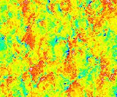
Anodized Aluminum Surface Texture Effect On Luster
Anodizing is an electrolytic passivation process commonly applied to convert aluminum to aluminum oxide. It can modify the surface texture and changes the microstructure of the metal near the surface. Such an anodized aluminum oxide layer is generally much stronger and more adherent than most types of paint and metal plating. It can significantly enhance corrosion and wear resistance and improve cosmetic effects of the products. Anodized aluminum is widely used on electronic devices and consumer products, such as cell phones, cameras, mp3 players and many others.
Here are examples of materials we tested this month:
Mechanical:
• Nanoindentation & scratch of tungsten carbide coatings
• Nanoindentation DMA of fluoropolymer
• Microindentation & scratch of DLC coatings
• Macro scratch firearm parts
3D Non-Contact Profilometry:
• Roughness of precision machined components
• Texture of textile samples
• Coplanarity of ball grid arrays
• Volume loss of dental samples
• Flatness measurement of micro seals
Tribology:
• Wear resistance of hard polymers
• Wear resistance of firearm parts
• High temperature fretting of engine parts
• Stribeck Curve of lubricants

3D Topography With Image Overlay of PCB
The more sophisticated electronic design and layout of semiconductor chips, circuits and systems requires high precision manufacturing and superior quality control. Unlike other techniques such as touch probes or interferometry, the Nanovea 3D Non-Contact Profilometer, using axial chromatism, can measure nearly any material surface. Nano through macro range is obtained during surface profile measurement with zero influence from sample reflectivity, absorption and high surface angles. This is ideal for surface inspection of the PCB assembly (PCBA), which contains a variety of electronic components of different materials, reflectivity and fine features. Moreover, the non-contact profiling technique measures the surface features without touching the PCBA, avoiding the risk of damaging the delicate circuits and electronic components due to sliding of the probe stylus. The combination of high precision, high speed, non-contact and user friendliness makes the Nanovea Profilometer an ideal tool for PCBA inspection.


