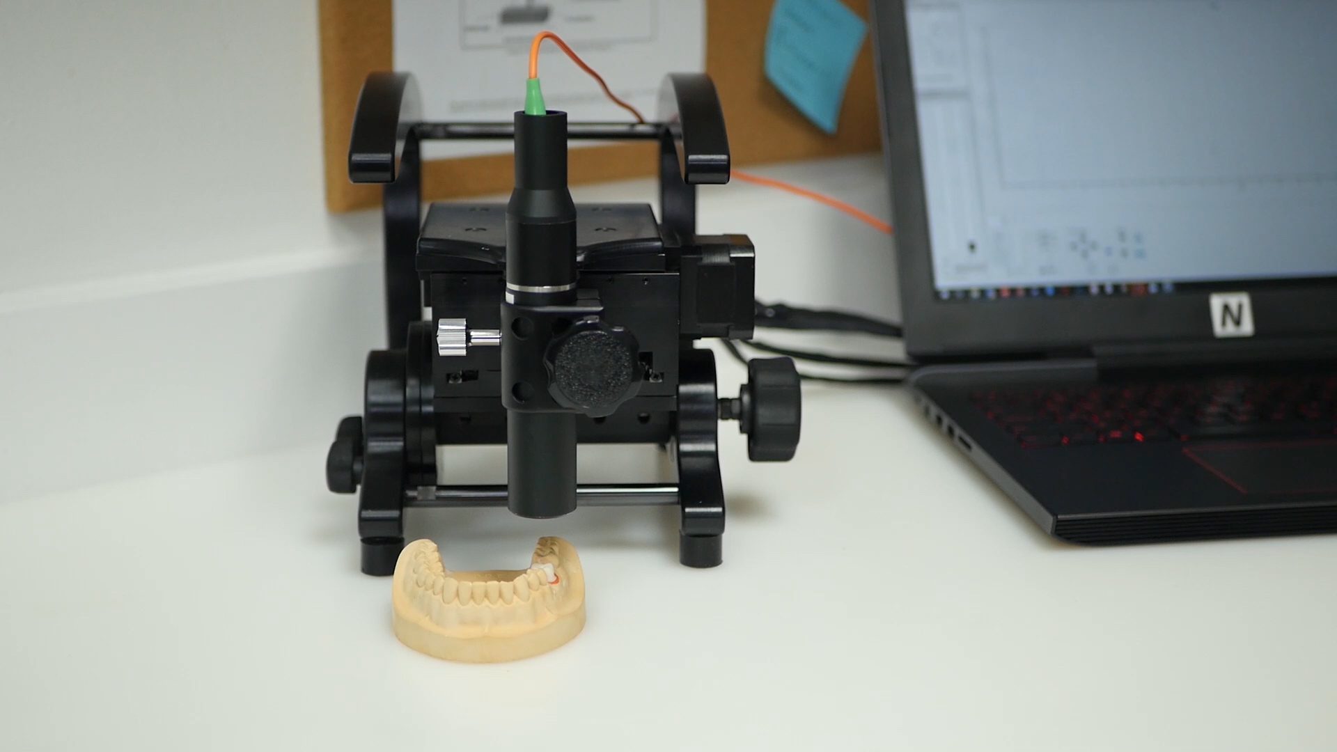
Understanding and quantifying a sample’s surface is crucial for many applications including quality control and research. To study surfaces, profilometers are often used to scan and image samples. A large problem with conventional profilometry instruments is the inability to accommodate for non conventional samples. Difficulties in measuring non conventional samples can occur due to sample size, geometry, inability to move the sample, or other inconvenient sample preparations. Nanovea’s portable 3D non-contact profilometers, the JR series, is able to solve most of these problems with its ability to scan sample surfaces from varying angles and its portability.
Categories
- Application Notes
- Block on Ring Tribology
- Corrosion Tribology
- Friction Testing | Coefficient of Friction
- High Temperature Mechanical Testing
- High Temperature Tribology
- Humidity and Gases Tribology
- Humidity Mechanical Testing
- Indentation | Creep and Relaxation
- Indentation | Fracture Toughness
- Indentation | Hardness and Elastic
- Indentation | Loss and Storage
- Indentation | Stress vs Strain
- Indentation | Yield Strength and Fatigue
- Laboratory Testing
- Linear Tribology
- Liquid Mechanical Testing
- Liquid Tribology
- Low Temperature Tribology
- Mechanical Testing
- Press Release
- Profilometry | Flatness and Warpage
- Profilometry | Geometry and Shape
- Profilometry | Roughness and Finish
- Profilometry | Step Height and Thickness
- Profilometry | Texture and Grain
- Profilometry | Volume and Area
- Profilometry Testing
- Ring on Ring Tribology
- Rotational Tribology
- Scratch Testing | Adhesive Failure
- Scratch Testing | Cohesive Failure
- Scratch Testing | Multi-Pass Wear
- Scratch Testing | Scratch Hardness
- Scratch Testing Tribology
- Tribology Testing
- Uncategorized
Archives
- March 2026
- November 2025
- September 2023
- August 2023
- June 2023
- May 2023
- July 2022
- May 2022
- April 2022
- January 2022
- December 2021
- November 2021
- October 2021
- September 2021
- August 2021
- July 2021
- June 2021
- May 2021
- March 2021
- February 2021
- December 2020
- November 2020
- October 2020
- September 2020
- July 2020
- May 2020
- April 2020
- March 2020
- February 2020
- January 2020
- November 2019
- October 2019
- September 2019
- August 2019
- July 2019
- June 2019
- May 2019
- April 2019
- March 2019
- January 2019
- December 2018
- November 2018
- October 2018
- September 2018
- July 2018
- June 2018
- April 2018
- March 2018
- February 2018
- November 2017
- October 2017
- September 2017
- August 2017
- June 2017
- May 2017
- March 2017
- February 2017
- January 2017
- November 2016
- October 2016
- August 2016
- July 2016
- June 2016
- May 2016
- April 2016
- March 2016
- February 2016
- January 2016
- December 2015
- November 2015
- October 2015
- September 2015
- August 2015
- July 2015
- June 2015
- May 2015
- April 2015
- March 2015
- February 2015
- January 2015
- November 2014
- October 2014
- September 2014
- August 2014
- July 2014
- June 2014
- May 2014
- April 2014
- March 2014
- February 2014
- January 2014
- December 2013
- November 2013
- October 2013
- September 2013
- August 2013
- July 2013
- June 2013
- May 2013
- April 2013
- March 2013
- February 2013
- January 2013
- December 2012
- November 2012
- October 2012
- September 2012
- August 2012
- July 2012
- June 2012
- May 2012
- April 2012
- March 2012
- February 2012
- January 2012
- December 2011
- November 2011
- October 2011
- September 2011
- August 2011
- July 2011
- June 2011
- May 2011
- November 2010
- January 2010
- April 2009
- March 2009
- January 2009
- December 2008
- October 2008
- August 2007
- July 2006
- March 2006
- January 2005
- April 2004


