USA/GLOBAL: +1-949-461-9292
EUROPE: +39-011-3052-794
CONTACT US

Roughness Mapping Inspection using 3D Profilometry

ROUGHNESS MAPPING INSPECTION

USING 3D PROFILOMETRY

Prepared by

DUANJIE, PhD

INTRODUCTION

Surface roughness and texture are critical factors that impact the final quality and performance of a product. A thorough understanding of surface roughness, texture, and consistency is essential for selecting the best processing and control measures. Fast, quantifiable, and reliable inline inspection of product surfaces is in need to identify the defective products in time and optimize production line conditions.

IMPORTANCE OF 3D NON-CONTACT PROFILOMETER FOR IN-LINE SURFACE INSPECTION

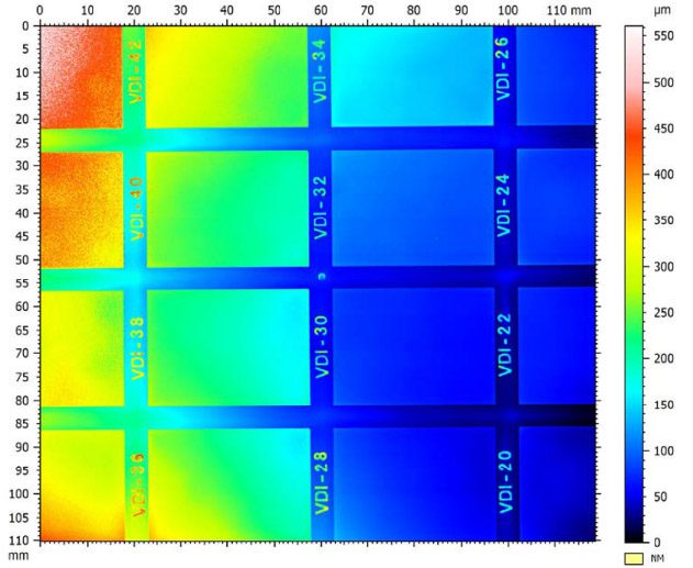
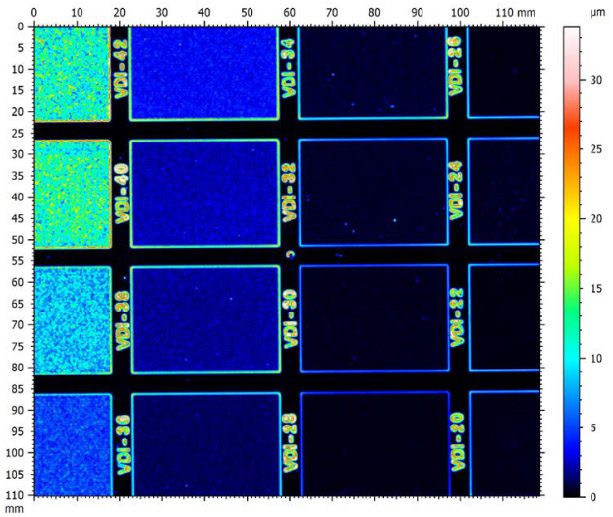
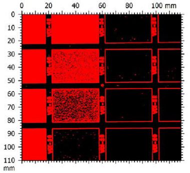
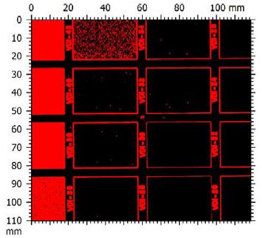
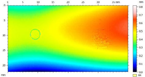
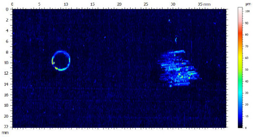
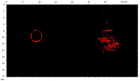
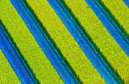
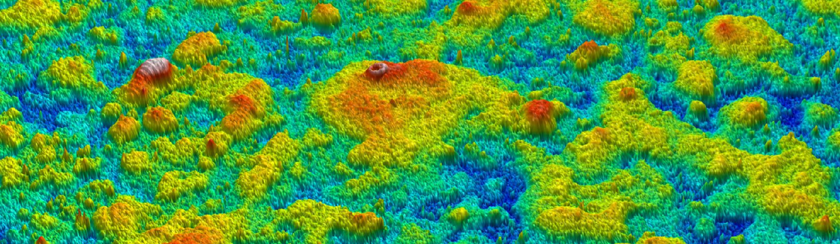
Surface defects in products result from materials processing and product manufacturing. Inline surface quality inspection ensures the tightest quality control of the end products. NANOVEA 3D Non-Contact Optical Profilers utilize Chromatic Light technology with unique capability to determine the roughness of a sample without contact. The line sensor enables scanning of the 3D profile of a large surface at a high speed. The roughness threshold, calculated in real-time by the analysis software, serves as a fast and reliable pass/fail tool.

MEASUREMENT OBJECTIVE

In this study, the NANOVEA ST400 equipped with a high-speed sensor is used to inspect the surface of a Teflon sample with defect to showcase the capability of NANOVEA

Non-Contact Profilometers in providing fast and reliable surface inspection in a production line.

NANOVEA

ST400

RESULTS & DISCUSSION

3D Surface Analysis of the Roughness Standard Sample

The surface of a Roughness Standard was scanned using a NANOVEA ST400 equipped with a high-speed sensor that generates a bright line of 192 points, as shown in FIGURE 1. These 192 points scan the sample surface at the same time, leading to significantly increased scan speed.

FIGURE 2 shows false color views of the Surface Height Map and Roughness Distribution Map of the Roughness Standard Sample. In FIGURE 2a, the Roughness Standard exhibits a slightly slanted surface as represented by the varied color gradient in each of the standard roughness blocks. In FIGURE 2b, homogeneous roughness distribution is shown in different roughness blocks, the color of which represents the roughness in the blocks.

FIGURE 3 shows the examples of the Pass/Fail Maps generated by the Analysis Software based on different Roughness Thresholds. The roughness blocks are highlighted in red when their surface roughness is above a certain set threshold value. This provides a tool for the user to set up a roughness threshold to determine the quality of a sample surface finish.

FIGURE 1: Optical line sensor scanning on the Roughness Standard sample

a. Surface Height Map:

b. Roughness Map:

FIGURE 2: False color views of the Surface Height Map and Roughness Distribution Map of the Roughness Standard Sample.

FIGURE 3: Pass/Fail Map based on the Roughness Threshold.

Surface Inspection of a Teflon Sample with Defects

Surface Height Map, Roughness Distribution Map and Pass/Fail Roughness Threshold Map of the Teflon sample surface are shown in FIGURE 4. The Teflon Sample has a ridge form at the right center of the sample as shown in the Surface Height Map.

a. Surface Height Map:

The different colors in the pallet of FIGURE 4b represents the roughness value on the local surface. The Roughness Map exhibits a homogeneous roughness in the intact area of the Teflon sample. However, the defects, in the forms of an indented ring and a wear scar are highlighted in bright color. The user can easily set up a Pass/Fail roughness threshold to locate the surface defects as shown in FIGURE 4c. Such a tool allows users to monitor in situ the product surface quality in the production line and discover defective products in time. The real-time roughness value is calculated and recorded as the products pass by the in-line optical sensor, which can serve as a fast but reliable tool for quality control.

b. Roughness Map:

c. Pass/Fail Roughness Threshold Map:

FIGURE 4: Surface Height Map, Roughness Distribution Map and Pass/Fail Roughness Threshold Map of the Teflon sample surface.

CONCLUSION

In this application, we have shown how the NANOVEA ST400 3D Non-Contact Optical Profiler equipped with an optical line sensor works as a reliable quality control tool in an effective and efficient manner.

The optical line sensor generates a bright line of 192 points that scan the sample surface at the same time, leading to significantly increased scan speed. It can be installed in the production line to monitor the surface roughness of the products in situ. The roughness threshold works as a dependable criteria to determine the surface quality of the products, allowing users to notice the defective products in time.

The data shown here represents only a portion of the calculations available in the analysis software. NANOVEA Profilometers measure virtually any surface in fields including Semiconductor, Microelectronics, Solar, Fiber Optics, Automotive, Aerospace, Metallurgy, Machining, Coatings, Pharmaceutical, Biomedical, Environmental and many others.

NOW, LET'S TALK ABOUT YOUR APPLICATION

Comment