Here are examples of materials we tested this month:
Mechanical:
• Nanoindentation oscillation of thin films
• Nanoindentation of peened surface
• Nano yield strength of mems
• Nano scratch of stent
• Nano scratch of microstrip
• Nano wear of implant
• Micro scratch of aluminum parts
3D Non-Contact Profilometry:
• Profile of micro machined surface
• Profile of anodization surface
• Planarity of micro marks
• Roughness of peened surface
• Topography of wood surface
• Step height of micro channel
• Step height of printed electronics
Tribology:
• Friction testing of silicon
• Ptfe coating wear friction testing
• 36hr wear rate of dlc coating
• Wear resistance of glass
• High temp wear resistance of graphite
Here are examples of materials we tested this month:
Mechanical:
• Nano fracture of ceramic
• Nano scratch of microelectronic coating
• Nano scratch of medical coating
• Nano compression of micro feature
• Nano stress strain solar film
• Micro scratch of TiN coating
• Microindentation of concrete
3D Non-Contact Profilometry:
• Texture patterns of fracture
• Flatness of flip chip
• Planarity of microelectronic
• Profile of dental samples
• Roughness of micro pitting
• Roughness of micro medical parts
• Step Height of solder paste
• Coefficient of friction polyurethane coating
• Coefficient of friction medical plastic
• 24hr Wear resistance of coated glass
• Wear resistance of submerged implant
• chrome carbide coating wear resistance
Here are examples of materials we tested this month:
Mechanical:
• Nano scratch of composite foil
• Nano scratch of composite samples
• Nano scratch of hard polymer
• Nano wear of implant
• Nanoindentaion of wafer samples
• Mechanical properties of laser welds with Nanoindentation
• Microindentation of rock
3D Non-Contact Profilometry:
• Roughness of print rollers
• Roughness of micro cones
• Roughness of dental implants
• Topography of laser etched polymer
• Flatness of ceramic samples
• Height variations of micro bumps
• Coplanarity of tool bit surface
• Depth consistency of micro channels
Tribology:
• Coefficient of friction powders
• Coefficient of friction gels
• Coefficient of friction grip samples
• Wear resistance of engine parts
• Wear resistance of hard fiber
• Wear resistance of hard glass composite
Here are examples of materials we tested this month:
Mechanical:
• Nano scratch of solar film
• Nano scratch of micro wires
• Nano wear of composite seals
• Nanoindentaion of wafer samples
• Nanoindentation of mineral particles
• Nano Compression of silicon
• Micro Fracture Toughness of carbon
3D Non-Contact Profilometry:
• Roughness of thin clear plastic
• Roughness of o-ring
• Sandblasted steel texture measurement
• Dimension of micro component
• Topography of rock drill head
• Profile of micro features
• Step Height of thin films
• CoPlanarity of samtec connector
Tribology:
• Coefficient of friction polished concrete
• Coefficient of friction elastomer
• Wear resistance of hard plastic casing
• Wear resistance of hard carbon coating
• Wear resistance of epoxy coating
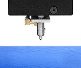
The Release of the Jr25 True Portable Profilometer
Nov, 2010 (Irvine, CA) – The Nanovea Jr25, 3D Non Contact Portable Profilometer, is the first truly portable high performance Profilometer of its kind. With an optional battery pack and carrying case, the Jr25 provides measurement capability rarely available during field study. The Jr25 is designed to easily utilize leading edge optical pens using superior white light axial chromatism measurement. Nano through macro range can be obtained during measurement (Profile/Dimension, Roughness/Finish/Texture, Shape/Form/Topography, Flatness/Warpage, Volume Area, Step-Height/Depth/Thickness and others) on a wider range of geometries and materials than any other Profilometer and now with true portable capability. With a total weight less than 5.5 Kg, the operator can safely place the Jr25 onto the surface under inspection. The Jr25 has the ability to measure an area up to 25mm x 25mm, and depending on the optical pen a depth up to 27mm and resolution down to 5nm. Focusing of the surface is achieved manually with a smooth touch micrometer and 30 mm travel range. Surfaces of almost any type can be measured regardless of how reflective/no reflective, transparent/opaque, or specular/diffusive the material is. With a fully rotational, single axis, head the Jr25 has the ability to measure surfaces at difficult angles. Along with quick and ease of use, the Jr25 has been designed specifically for production environments where samples cannot be moved and open field studies. “The door has now been opened for our 3D Non Contact technique to reach environments untouched by this type of measurement ability; from the moon to the desert and everything in between. The field has truly become the lab with this type of measurement resource at your side.” – Craig Leising | Product Manager
US Nanotechnology Instrument Manufacturer Proves the Success of R&D Stimulus
Irvine CA, Jan 25, 2010 – Like many throughout the country, you may be asking how the billions poured into science R&D has helped stimulate our economy. Well, look no further than the nanotechnology instrument manufacture, Nanovea based in Irvine, CA. 2009 just ended as their first branded year with new hires, new instruments and more business to send to their local machine shops and parts suppliers. From their Irvine, CA office Nanovea designs and manufactures 3D Profilometers, Mechanical Testers & Tribometers to combine the most advanced testing capabilities in the industry:Scratch, Adhesion, Hardness, Wear, Friction & 3D Non-Contact Metrology at Nano, Micro & Macro range. Unlike other manufactures Nanovea also provides Laboratory Services, offering clients availability to the latest technology and optimal results through improvements in material testing standards. So what does Nanovea have to do with the stimulus given to research in the United States? Well coincidently, everything and here’s how. The stimulus given to research labs, universities and companies was intended for the development of new innovations and materials to support growing industries such as solar, energy, biomedical etc. To create new, and or improve, material requires new instruments to measure and insure material characteristics during research and development. Then, instrumentation would also be needed to monitor the mass development of these new materials for quality control. Nanovea had been designing and manufacturing instruments for this very purpose since 2004 and had been preparing for a brand launch at the end of 2008. With the direction of a newly hired marketing manager Nanovea prepared its launch in one of the most challenging economic times the US may have ever faced. Nanovea embraced the challenge and took full advantage of the needs of the research community both in the US and Internationally. With three clear product lines and services Nanovea provided solutions throughout 2009 to high growth industries in need of nano through macro scale measurement needs. Now 2010 has already begun with several new projects throughout the world and with local solar, pharmaceutical and medical clients throughout California. “Being a US manufacturer of nano instruments and services during this time has provided us with some great opportunities to establish our brand. We are very thankful and also very proud that were able to support the economy with new hires and business to our local partners.” —Pierre Leroux, Nanovea President | Ceo
Nanometer Online Inspection With Nanovea 3D Non-Contact Profilometer
Irvine CA, Jan 05, 2010 – Nanovea 3D Non-Contact Profilometer will now have optional online capability for automated inspection and report generation. With this advancement Nanovea’s Profilometer can now effortlessly integrate into large or small quality control environments. Crucial applications throughout all industries, which were once inspected with vision and or touch-probe, will now be inspected with the assurance of high speed noncontact nanometer measurement. This is especially critical to batch production with tight tolerance levels which can now be easily monitored to insure quality control via online communication. With this new feature applications can be automatically scanned and analyzed based on instructions found on a server database. The online inspection feature allows automatic product ID scan with a bar code reader (could also be manually entered in); the product ID is then checked against predefined pass/fail and measurement requirements stored on a company database. The part is automatically measured, and upon completion a report is automatically generated. The report and the pass/fail information is automatically sent back to the server and stored with that part number. Measurement speeds range from 1m/s and 31,000 points/sec with nanometer accuracies. There are various scan types, analysis functions and size options that can be customized to fit applications throughout all industries. “This is a very exciting capability for Nanovea. Our Profilometers can best utilize online inspection at this time, but it is also a new option for our Mechanical Testers when hardness could be used for quality control.”
—Craig Leising, Product Manager
Breakthrough Nanoindentation Testing With Image Pattern Recognition
Irvine CA, April 1, 2009 – Nanovea announced today a breakthrough development in Nanoindentation testing by combining advanced image pattern recognition capabilities to the most advanced nano-indenter for quality control applications. Nanovea has now combined their, PRVision, machine vision camera option to Nanoindentation testing that allows auto-recognition of precisely chosen features with little to no user interaction. The user-friendly software of Nanovea’s PRVision allows for an automatic test of hardness and elastic modulus on patterned samples or specifically chosen areas of interest. Nanoindentation properties including hardness and elastic modulus can then be automatically measured and recorded. The “quasi non-destructive” low loads associated with Nanoindentation Testing makes this technique an ideal breakthrough tool to monitor the quality control of environments where hardness and elastic modulus are crucial: Micro Electronics, Solar, Pharmaceuticals and many others. “Nanoindentation until now was performed using primitive mapping options. Our PRVision option will speed up Nanoindentation testing and opens the door to wide-scale automatic production quality control applications where hardness and elastic modulus are the best control parameters.” Said Pierre Leroux, CEO/President, Nanovea.
Top Semiconductor Mfg Chooses Nanovea Profilometer Over Many
Irvine CA, March 5, 2009 – Nanovea announced today that it will ship a top Semiconductor Mfg its first HS1000 Profilometer. The HS1000 delivery adds yet another highlight to Nanovea’s impressive Optical Profiler history and offers customers a more advanced measurement speed option for high throughput demands. The HS1000 Profilometer is equipped with an unmatched combination of measurement speed, automation and nanometer resolution.Until the Nanovea HS1000 Profilometer, full automation and the unique advantages of white-light axial chromatism technique were features rarely found in a single high scanning speed instrument; a feature the Client requested and only Nanovea could deliver. Traditional high speed instruments would typically sacrifice one feature for another, speed or resolution, which limited the users overall measurement capability. The HS1000 Profilometer stage speed can reach 1m/s, up to 50 times faster than most optical profilers in its class. The HS1000 Profilometer is equipped with a 31KHz white-light axial chromatism sensor and XY measurement area of 400mm x 600mm, which at maximum stage speed can measure 1 point every 32µm and traverse the full 400mm in less than 1 sec. (higher resolution can be obtained with proportionally slower stage speeds). In addition, the HS1000 Profilometer has a machine vision camera option that allows auto-recognition on precisely chosen surface features with little to no user interaction. The user-friendly software and the optional machine vision camera allows for an automatic scan of the surface to recognize all features of interest. These features can then be automatically measured or the user can select from a list from which to measure. The combination of superior overall features makes the HS1000 Profilometer unquestionably the instrument of choice for high throughput demands found in Semiconductor, Solar and Pharmaceutical industries. “It goes without saying the importance of gaining this client’s choice. I’m proud of our team’s ability to deliver with such an important opportunity,” Said Craig Leising, Product Manager, Nanovea.
Nanovea Profilometer Receives “Class 1”Cleanroom Approval
Irvine, CA, January 22, 2009 — Nanovea Inc. announced today the successful installation of their Profilometer within the Class 1 Cleanroom of a leading micro-electronics manufacturer. Class 1 Cleanroom clearance is known for its strict compliance and custom demand for all materials used in the development of the instrument. The advanced 3D non-contact profiling abilities of Nanovea’s Profilometers will now be an option for the strictest microelectronic cleanroom requirements. With the use of “clean” motorized linear stages and the proper selection of materials, Nanovea’s engineers custom designed a system that would be compatible with the strict class 1 standards. Class 1 Cleanrooms have a tightly controlled level of contamination and allows for very few particles of any kind. The material selection was crucial in the design of the X-Y stages so that few particles are emitted into the air during testing. The system was also designed with a high degree of flatness, accuracy and with a level of automation that allows the user to measure multiple areas and stitch them together. This will allow the user to create one large, planar surface in order to compare relative flatness with very little user interaction. The measureable area of the custom profiler can be as large as 30cm x 30cm with vertical resolution down to 2nm. A design is also available to scan large, heavy and even immoveable parts. This is only a glimpse at the projects Nanovea’s engineers have customized. They have also provided a custom built high-speed Profilometer with speeds over 30,000 points/second and machine vision with image recognition to improve efficiency. Additionally, Profilometer have been built with custom scanning capabilities to acquire surface measurements from both the top and bottom surfaces while measuring the thickness of the material, all with nanometer resolution. “The addition of the cleanroom design will allow Nanovea to work closer with strict environments, and once again shows our dedication to ingenuity.” Said Craig Leising, Product Manager Nanovea, Inc.