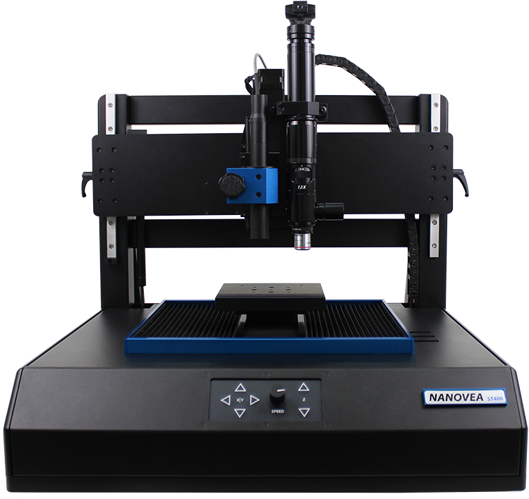
NANOVEA ST400 Modular 3D Surface Profiler

What makes NANOVEA 3D Surface Profilometers different?
SELECTED PROFILOMETRY APPLICATIONS:


BUILT FOR PROS
While competitors move toward “one-click,” consumer-grade tools, we stay true to the highest metrology standards. We confidently support those who prioritize accuracy and repeatability in their results.
Our instruments are developed by scientists and engineers who understand the complex demands of advanced materials research and industrial applications.
What does this mean for you?
EXPERT GUIDANCE
Our engineers collaborate with you to fully understand your application, ensuring the system perfectly aligns with your unique needs and goals.
CONFIDENCE IN RESULTS
Powered by White Light technology, our instruments measure physical wavelengths directly, instead of relying on algorithms to “interpret” features of the surface. This ensures your data is accurate, reliable and repeatable.
YOUR PARTNER IN INNOVATION
We help you grow! Our Profilometers are built with your challenges in mind – to help you solve complex problems, not just help your intern perform basic tasks. While others dumb things down, we support you in understanding your materials and expanding your expertise through comprehensive training, and – when needed – courses and consulting.
BUILT IN USA & ITALY
NANOVEA Profilometers are designed, developed AND built in-house at our HQ in Irvine, California and at NANOVEA EU in Turin, Italy.
What does this mean for you?
SUPERIOR QUALITY CONTROL
Every step of development and manufacturing is under our direct supervision, ensuring your instrument meets the highest standards of accuracy and reliability.
FASTER RESPONSE TIMES
In-house manufacturing allows for better communication, a personalized approach, and streamlined support whenever you need us.
PEACE OF MIND
You partner with a company that has been leading the industry since the early 2000s, with unparalleled expertise spanning industries, materials, and applications — from NASA to NIST.
BUILT TO ORDER
Unlike competitors who sell you off-the-shelf products at the same (or higher.. sometimes MUCH higher!) price, NANOVEA builds the instrument for you.
What does this mean for you?
STATE-OF-THE-ART AT NO EXTRA COST
Having our Development, Manufacturing and Support teams closely collaborating under one roof means years of perfecting our technology one instrument at a time. Based on global customer feedback, you always receive the latest version — without “novelty” pricing.
YOU GET WHAT YOU NEED, NOT WHAT'S EASIEST FOR US TO SELL
Getting an “in-stock” instrument might seem convenient but in reality, it means you’re dealing with salespeople whose only goal is to close the sale — not to ensure you get the right solution for your needs.
A LASTING INVESTMENT
Our modular systems are built to grow with you, reducing the need for frequent upgrades, minimizing downtime, and ensuring long-term value and satisfaction.