Category: Press Release

The Worlds First Dual Load Controlled Tribometer
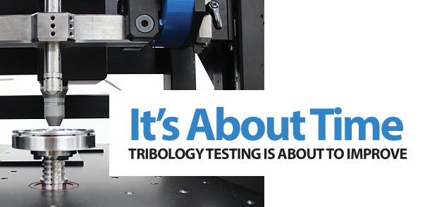
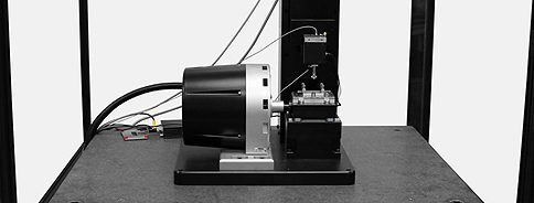
Irvine CA, February 28, 2018 – The Nanovea T2000 is the worlds first dual load controlled Tribometer providing vertical force oscillation at frequencies up to 150Hz. It combines advanced pneumatic technology with a state of the art linear electromagnetic stage to provide controlled loading from 1mN to 2000N during rotative and linear testing. Pneumatic is used from 5 to 2000N offering multiple advantages compared with age old spring/motor technologies used on other systems. With spring/motor technologies, the load sensor is typically placed behind the spring. This means that it is not measuring the actual variation of load applied on the surface during the test. The T2000 measures the load by a direct connection between the ball holder and the actual load cell. This ensures that the load measured is actually the load applied on the surface. The linear electromagnetic loading system of the T2000 can apply a vertical force of 0.2 to 20N at frequencies up to 150Hz. As an example, the normal load can be increased from 0 to100N with the pneumatic technology and then the linear motor can vary the load from 90 to 110N and up to 150 times per second. This gives the unique capability of superposing a control fatigue or vibration level to the main constant force applied by the pneumatic system. This electromagnetic linear stage can also apply directly very low loads from 1mN to 5N to complete the full range.
See Video Clip Discover more in the Application Note or visit Nanovea Tribómetros

In-line Inspection Game Changer
Using in-line inspection (POINT or LINE SENSORS) Nanovea’s unique in-line software package can measure and analyze “live” roughness and texture parameters meeting standards for up to 8 points sensors or up to 4 line sensors. The software has many features including pass and fail criteria specific to each sensor or average of all sensors. Acquisition rates of more than 1,300,000 points per seconds. This is ideal for any film/paper sheet measurements and other in-line applications. Nanovea provides integration support including specific mounting structure.

Cutting Tool Edge Measurement in Seconds
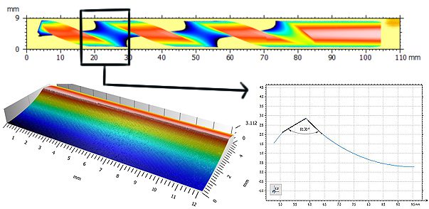
Irvine CA, July 27, 2016 – Conventional profilometry scans sample surfaces from a single, fixed direction. This is only appropriate for measuring sufficiently flat samples, as opposed to cylindrical shapes that require a precise 360° rotation. For an application such as characterizing the helical cutting edge of a tool, a conventional machine would need multiple scans from different angles of the entire part, as well as significant post scan data manipulation. This is often too time consuming for QC applications that only require measurements from very specific regions.
NANOVEA’S rotational stage solves this problem with simultaneous motion control of the lateral and rotational axes. This technique eliminates the time consuming need of measuring the entire part and continuous realignment. Instead, the full circumference of the entire cutting edge can be determined in seconds. All desired angles and features can be directly determined from the scan, with no need for the extensive stitching together of multiple files.
NANOVEA’s chromatic confocal technique offers far greater resolution, down to 2.7 nm, and accuracy than Focus Variation competitors. The raw surface height is measured directly from the detection of the wavelength focused on the surface, with none of the errors caused by Interferometry techniques, no field of view limitations, and no need for sample surface preparation. Materials with extremely high or low reflectivity can easily be measured and very high wall angles are accurately characterized without any issue.
Coupled with NANOVEA’s line sensor, a bar of data up to 4.78mm wide can be captured in a single pass, while moving linearly for up to 150mm in the scanning direction. Simultaneously, the rotational stage can revolve the sample at the desired speed. Put together, this system allows for the creation of a continuous 3D height map of the entire circumference of a cutting edge, with any pitch or radius, in a fraction of the time when compared to other technologies.
See App Note: Rotational Measurement Using 3D Profilometry
Breakthrough Indentation Yield Strength Test by Nanovea
Irvine CA, July 14, 2011 – Nanovea today introduced its patent pending breakthrough method of reliably acquiring yield strength through indentation; ultimately replacing the traditional tensile testing machine for yield strength measurement. Traditionally yield strength has been tested by using a tensile testing machine, a large instrument requiring enormous strength to pull apart metal, plastic and others. The yield strength (also known as yield point) of a material in engineering (and or materials science) is the point of stress that a material starts to deform plastically. Before reaching the yield point a material will deform elastically but returns to its original shape when stress is removed. A crucial material property for nano and micro related materials found in advancing industries such as biomedical, microelectronics, energy and many others. Until now the most reliable way took large machine effort, sample preperation, and or was impossible to perform on small samples and localized areas. By using Nanovea’s Mechanical Tester in indentation mode, using a cylindrical flat tip, yield strength data can be easily obtained. For years now, the indentation test has been used for hardness and elastic modulus measurements. There has traditionally been an issue with linking macro tensile properties to what was measured during an indentation test. Many studies measuring with spherical tips have allowed stress-strain curves but were never able to give reliable tensile yield strength data that corresponded directly to macro tensile data. Nanovea’s patent pending method, using a cylindrical flat tip, gives yield strength directly comparable to what is measured by traditional means. It is believed that the load per surface area at which the cylindrical flat tip penetrates, at increased speed, is directly linked to the load versus surface area at which the material starts flowing in a tensile mode test. Therefore, reliable yield strength results on an endless list of materials, small or large has never before been as obtainable until now. “This is just another addition, on a long and growing list, of what can be tested with our Mechanical Tester,” said Pierre Leroux, Nanovea’s CEO. While this specific test is a breakthrough of great importance, it is ultimately just another reason why the Nanovea Mechanical Tester has the widest testing capability of any mechanical testing system.
For application note visit: Breakthrough Indentation Yield Strength Testing
Avance en las pruebas de nanodesgaste a alta velocidad
20 de febrero de 2013 - Irvine (California) - Nanovea ha anunciado hoy la finalización de un sistema de pruebas de desgaste nanométrico capaz de alcanzar velocidades de hasta 1400 mm/seg. La longitud única de la carrera, de hasta 10 mm, combinada con un movimiento lineal a una velocidad de hasta 70 Hz, y posiblemente a frecuencias más altas, permite velocidades nunca antes disponibles para Nano Wear Testing.
Los instrumentos de ensayo de desgaste existen desde hace más de medio siglo. Desde el principio, las cargas de ensayo solían ser superiores a 1N y las velocidades eran lentas, excepto en las aplicaciones de rozamiento más recientes, en las que el desplazamiento se limitaba a decenas de micras. La nanoindentación apareció a finales de los 80 con la capacidad de proporcionar cargas mucho más bajas. Los primeros sistemas estaban, y siguen estando en su mayoría, basados en un sistema de bobina sin bucle de control de realimentación. El bucle de control de realimentación es esencial para proporcionar un control superior de la carga cuando se mueve la posición del contacto, como es el caso de los ensayos de rayado o desgaste. Los ensayos de nano rayado con combinación de célula de carga piezoeléctrica aparecieron a finales de los años 90. Los primeros sistemas utilizaban tecnologías cantilever que daban suficiente velocidad al control de retroalimentación durante los ensayos de rayado y desgaste, pero la velocidad de desplazamiento estaba, y sigue estando, limitada a menos de 10 mm/seg. Para muchas aplicaciones, la vida útil requiere un número muy elevado de ciclos para garantizar que el dispositivo resistirá tras años de uso. Con la lenta velocidad de que disponen las tecnologías cantilever, podrían necesitarse más de 6 meses para realizar una sola prueba de desgaste. Esto es poco práctico y ralentiza claramente el desarrollo y la aprobación de nuevas tecnologías.
Nanovea es capaz de alcanzar velocidades más rápidas y un control seguro de las cargas durante los ensayos de desgaste Nano utilizando un sistema de altavoces de bobina para un desplazamiento rápido y suave. Añadiendo el uso del Nanovea Nano Módulo con un actuador piezoeléctrico y una célula de carga ultrasensible crea un control de carga rápido con montaje vertical para garantizar una respuesta superior a la velocidad.
"Tuvimos la oportunidad de demostrar la capacidad de nuestro equipo con este proyecto. Estamos muy orgullosos de este logro. Esta nueva tecnología acelerará la introducción de nuevos dispositivos con mayor vida útil en el mercado de clientes." -CEO, Pierre Leroux

High Speed Nanotribology Testing Breakthrough
Feb 21, 2013 – Irvine, CA – Nanovea announced today the completion of a Nanotribology System capable of speeds as high as 1400mm/sec. The unique length of stroke, up to 10mm, combined with a linear movement at a rate up to 70Hz, and possibly at higher frequencies, allows speeds never before available for Nano Wear Testing.
Los instrumentos de ensayo de desgaste existen desde hace más de medio siglo. Desde el principio, las cargas de ensayo solían ser superiores a 1N y las velocidades eran lentas, excepto en las aplicaciones de rozamiento más recientes, en las que el desplazamiento se limitaba a decenas de micras. La nanoindentación apareció a finales de los 80 con la capacidad de proporcionar cargas mucho más bajas. Los primeros sistemas estaban, y siguen estando en su mayoría, basados en un sistema de bobina sin bucle de control de realimentación. El bucle de control de realimentación es esencial para proporcionar un control superior de la carga cuando se mueve la posición del contacto, como es el caso de los ensayos de rayado o desgaste. Los ensayos de nano rayado con combinación de célula de carga piezoeléctrica aparecieron a finales de los años 90. Los primeros sistemas utilizaban tecnologías cantilever que daban suficiente velocidad al control de retroalimentación durante los ensayos de rayado y desgaste, pero la velocidad de desplazamiento estaba, y sigue estando, limitada a menos de 10 mm/seg. Para muchas aplicaciones, la vida útil requiere un número muy elevado de ciclos para garantizar que el dispositivo resistirá tras años de uso. Con la lenta velocidad de que disponen las tecnologías cantilever, podrían necesitarse más de 6 meses para realizar una sola prueba de desgaste. Esto es poco práctico y ralentiza claramente el desarrollo y la aprobación de nuevas tecnologías.
Nanovea is able to attain faster speeds and secure control of the loads during Nano Wear Testing by using a coil speaker system for quick and smooth displacement. Adding the use of the Nanovea Nano Module with a piezo actuator and an ultra-sensitive load cell creates a quick load control with vertical mounting to ensure superior response to speed.
“We were given the opportunity to really prove our team’s capability here with this project. We are very proud of this achievement. This new technology will speed up the introduction of new devices with increased service life to the customer market.” –CEO, Pierre Leroux
Nanovea Unveils Its New Revolutionary N3 Line
Irvine CA, January 18, 2012 – Nanovea today announced the arrival of the N3 line dedicated to providing high-end measurement technology to the broader market. Nanovea has fully automated their measurement techniques while designing to price in the $20K market.
The headline of the N3 line is the M3, a breakthrough in technology that aims at two distinct aspects missing in the hardness testing market. First, the combination of three factors never before available: nanometer range, controlled load & depth and a competitive price to compete in the $20K market. This provides universities and smaller R&D units to affordable nanoindentation capability. The M3 introduces an entirely new user capability with this price range, providing affordable access too quick and easy nanoindentation results under ASTM standard. Second, is to offer next generation technology to replace the traditional Visual Micro Vickers Hardness Testers that have not changed in more than 15 years. To achieve this, the indentation method has been made fully automated with no need to visually observe the indent which eliminates user error or problems with image recognition software that may have issues with material color and texture. Also, this new technology can achieve lower load and will work on thin coatings and all ranges of materials including ceramics, polymers, metals and others. The fully automated system has a touch screen start that gives automatic average of multiple measurements in minutes. The unit is compact and fully contained with only one standard electrical cable to connect. Because of these advancements in technology and the very competitive price, the M3 line will be the replacement of choice for older Micro Vickers Tester currently used in industrial high throughput quality control environments.
The M3 ushers in a new era of hardness testing by providing measurement capability that until this point targeted very specifically high end research. Essentially, like most technological advancements, price has kept nanoindentación capability out of the reach of the broader market still using standard hardness testing equipment. The M3 will be a significant replacement at an affordable cost and the result will be revolutionary. But Nanovea didn’t stop there. The M3 is only one of three new products from Nanovea’s new N3 line. Along with the M3 Nanovea also introduces the P3 and the T3.
The P3 is a significant advancement with 3D non contact metrology, providing automatic nanometer ISO roughness and step data on nearly any material; a capability unavailable in the 20k market. The P3 will provide to a broader market in need of automatic nano through macro roughness data without the high cost associated with a complete Profilometer system. And last but not least, the T3, like the P3 was developed to provide quick, easy and affordable access to high end measurement capability. The T3 is an automatic nano wear tester using linear reciprocating, ASTM g133, for wear rate study.
“The N3 line is a revolution of high end material measurement instruments, each in their own way and in their own markets. Each has been strategically designed to follow Nanovea’s goal to provide crucial nanotechnology to the broader market. As with many technologies being developed today to advance our society, price will ultimately control broad acceptance and use. It is no different with measurement technology and is just as crucial if not more.” said Pierre Leroux, Nanovea’s CEO.
Nanovea will be releasing the N3 line for the first time publicly at the Fall 2012 MRS show. Purchase orders for the N3 line begin in April for delivery in June 2012.
The Release of the Jr25 True Portable Profilometer
Nov, 2010 (Irvine, CA) – The Nanovea Jr25, 3D Non Contact Portable Profilometer, is the first truly portable high performance Profilometer of its kind. With an optional battery pack and carrying case, the Jr25 provides measurement capability rarely available during field study. The Jr25 is designed to easily utilize leading edge optical pens using superior white light axial chromatism measurement. Nano through macro range can be obtained during measurement (Profile/Dimension, Roughness/Finish/Texture, Shape/Form/Topography, Flatness/Warpage, Volume Area, Step-Height/Depth/Thickness and others) on a wider range of geometries and materials than any other Perfilómetro and now with true portable capability. With a total weight less than 5.5 Kg, the operator can safely place the Jr25 onto the surface under inspection. The Jr25 has the ability to measure an area up to 25mm x 25mm, and depending on the optical pen a depth up to 27mm and resolution down to 5nm. Focusing of the surface is achieved manually with a smooth touch micrometer and 30 mm travel range. Surfaces of almost any type can be measured regardless of how reflective/no reflective, transparent/opaque, or specular/diffusive the material is. With a fully rotational, single axis, head the Jr25 has the ability to measure surfaces at difficult angles. Along with quick and ease of use, the Jr25 has been designed specifically for production environments where samples cannot be moved and open field studies. “The door has now been opened for our 3D Non Contact technique to reach environments untouched by this type of measurement ability; from the moon to the desert and everything in between. The field has truly become the lab with this type of measurement resource at your side.” – Craig Leising | Product Manager
US Nanotechnology Instrument Manufacturer Proves the Success of R&D Stimulus
Irvine CA, Jan 25, 2010 – Like many throughout the country, you may be asking how the billions poured into science R&D has helped stimulate our economy. Well, look no further than the nanotechnology instrument manufacture, Nanovea based in Irvine, CA. 2009 just ended as their first branded year with new hires, new instruments and more business to send to their local machine shops and parts suppliers. From their Irvine, CA office Nanovea designs and manufactures 3D Perfilómetros, Mechanical Testers & Tribómetros to combine the most advanced testing capabilities in the industry:Scratch, Adhesion, Hardness, Wear, Friction & 3D Non-Contact Metrology at Nano, Micro & Macro range. Unlike other manufactures Nanovea also provides Laboratory Services, offering clients availability to the latest technology and optimal results through improvements in material testing standards. So what does Nanovea have to do with the stimulus given to research in the United States? Well coincidently, everything and here’s how. The stimulus given to research labs, universities and companies was intended for the development of new innovations and materials to support growing industries such as solar, energy, biomedical etc. To create new, and or improve, material requires new instruments to measure and insure material characteristics during research and development. Then, instrumentation would also be needed to monitor the mass development of these new materials for quality control. Nanovea had been designing and manufacturing instruments for this very purpose since 2004 and had been preparing for a brand launch at the end of 2008. With the direction of a newly hired marketing manager Nanovea prepared its launch in one of the most challenging economic times the US may have ever faced. Nanovea embraced the challenge and took full advantage of the needs of the research community both in the US and Internationally. With three clear product lines and services Nanovea provided solutions throughout 2009 to high growth industries in need of nano through macro scale measurement needs. Now 2010 has already begun with several new projects throughout the world and with local solar, pharmaceutical and medical clients throughout California. “Being a US manufacturer of nano instruments and services during this time has provided us with some great opportunities to establish our brand. We are very thankful and also very proud that were able to support the economy with new hires and business to our local partners.” —Pierre Leroux, Nanovea President | Ceo
Nanometer Online Inspection With Nanovea 3D Non-Contact Profilometer
Irvine CA, Jan 05, 2010 – Nanovea 3D Non-Contact Profilometer will now have optional online capability for automated inspection and report generation. With this advancement Nanovea’s Perfilómetro can now effortlessly integrate into large or small quality control environments. Crucial applications throughout all industries, which were once inspected with vision and or touch-probe, will now be inspected with the assurance of high speed noncontact nanometer measurement. This is especially critical to batch production with tight tolerance levels which can now be easily monitored to insure quality control via online communication. With this new feature applications can be automatically scanned and analyzed based on instructions found on a server database. The online inspection feature allows automatic product ID scan with a bar code reader (could also be manually entered in); the product ID is then checked against predefined pass/fail and measurement requirements stored on a company database. The part is automatically measured, and upon completion a report is automatically generated. The report and the pass/fail information is automatically sent back to the server and stored with that part number. Measurement speeds range from 1m/s and 31,000 points/sec with nanometer accuracies. There are various scan types, analysis functions and size options that can be customized to fit applications throughout all industries. “This is a very exciting capability for Nanovea. Our Profilometers can best utilize online inspection at this time, but it is also a new option for our Mechanical Testers when hardness could be used for quality control.”
—Craig Leising, Product Manager


