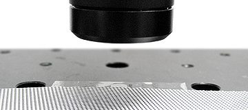
Flatness Measurement of Wafer Using 3D Profilometry
In this application the Nanovea ST400 Profilometer is used to measure the section of a wafer array. The area measured was selected at random, and assumed large enough in that it could be extrapolated to make assumptions about a much larger surface. Surface flatness measurement, planarity & other surface parameters are used to analyze the surface.


