Monthly Archives: April 2012
THE MEASUREMENT OF TRUTH. INTERFEROMETRY DISADVANTAGES
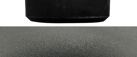
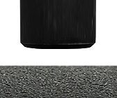
Some thoughts on what to consider when reviewing the two white light profilometer techniques. White Light Interferometry disadvantages start with using software and mathematical equations to detect, through the imaging system, the movement of fringes across the screen as the sample or the measuring head is moved up or down in specific steps. These measurements are only as as good as what the software and imaging parts can do in terms of “detecting” the movement of these fringes. When dealing with reflective and smooth surfaces, the accuracy of the data is superior. This is why the technique has been primarily developed for semiconductor applications where surfaces are often reflective and steps, if present, are close to 90° angles.
However, with a rough and low reflective surface, the software interpretation of the real surface becomes far from the truth because of inherent artifacts of the Interferometry technique. In addition to this, Interferometry is also extremely limited in terms of angle measurement. Again, software can now accomplish miracles to complete surfaces with additional information such as expected shape of surface. Previewing the raw data is one way to know what the software has manipulated but even the primary analysis software automatically renders an interpretation of what the surface must look like and automatically completes unmeasured points without the user knowing. With clever software, artifacts can be impossible to distinguish from real data since the rendering of the 3D image will look perfect and often users do not know what their surface really look like. This is especially true when dealing with more complex and difficult surfaces.
Also, speed is brought up as a major difference between the two techniques. It is true that Interferometry can more quickly measure one field of view image to evaluate roughness and step. These are clear advantages when dealing with smooth semiconductor surfaces. But again, if the surface being measured is not smooth the data may be provided more quickly but is far from true data. Additionally, stitching of surfaces works when, again, the surface is smooth and reflective and with clear position markers. The accuracy of stitching will reduce as the surface becomes rougher and with more difficult types of materials. It can become difficult to detect artifacts and issues with this when the surface is rougher than when you see a clear step. To obtain the best lateral resolution is it necessary to use a 100x objective, which limits the measurement area to approximately 140micrometer x 110 micrometer. The number of images to stitch can become a problem when trying to get accurate data on larger parts (100 images for 1mmx1mm and 10000 images for a 10mmx10mm). The lateral resolution of the image is a function of the number of pixels in the camera being used.
Unlike the manipulative Interferometry technique, White light Axial Chromatism technology measures height directly from the detection of the wavelength that hits the surface of the sample in focus. It is direct measurement with no mathematical software manipulation. This provides unmatched accuracy on the surface measured because a data point is either measured accurately without software interpretation or not at all. The software can complete the unmeasured point but the user is fully aware of it and can have confidence that there is no other hidden artifacts. The technique can also measure nearly any material surface with much higher angles up to over 80° in some cases. Axial Chromatism can scan on a length of over 30cm in less than 0.3 second. New acquisition system are now available to reach 31,000 points per second with 1m/s scanning. New line sensors with Axial Chromatism can actually measure up to 324,000points per second. A typical image acquired by an interferometer would have less than 1,000,000 data points per field of view. Using an Axial Chromatism line sensor scanning will take a few seconds which means that the actual speed is very close to Interferometry speeds while providing truer data. Therefore speed should be considered based on the application itself.
The growth of Interferometry technique was mostly due to their success in industries with deeper pockets. Therefore, the cost of Interferometry is generally twice that of Axial Chromatism systems with similar resolution and broader capability. It is our experience that 90% of applications are better served using the Axial Chromatism technique. Clients that have chosen Axial Chromatism technology have rarely been disappointed while there are many pitfalls with the choice of Interferometry. And the regret is almost always the same: Interferometry’s disadvantage of broad measurement capability and reliably true data with a high price tag.
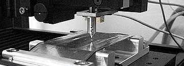
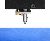
Nano Puncture Resistance Using Nanoindentation
In this application, the Nanovea Mechanical Tester, in Nanoindentation mode is used to study the puncture resistance of an aluminum foil sample using a cylindrical flat tip indenter. A custom sample holder was designed to secure thin film and foil samples.
Here are examples of materials we tested this month:
Mechanical:
• Nanoindentation of sicn coatings
• Nanoindentation stress-strain of polymer
• Nanoindentation yield strength of mems
• Nano Scratch of catheter coatings
• Nano Friction of rtil film
• Micro Scratch of tablet coatings
• Micro Wear of micro copper wire
3D Non-Contact Profilometry:
• Topography of fractured automotive part
• Dimension of ceramic micro features
• Roughness of pvc samples
• Roughness of plastic injection mold
• Flatness of glass samples
• Volume loss of wear tracks
Tribology:
• COF of various oil formulas
• COF of polymer medical tube
• Wear rate of rubber seal
• Wear rate of coil coatings
• Wear rate of carbon coated steel